
Manufacturing method and layout structure of back-illuminated sensor

A technology of layout structure and manufacturing method, which is applied to electric solid-state devices, semiconductor devices, radiation control devices, etc., can solve problems such as affecting the performance of back-illuminated sensor chips, uneven imaging, affecting the transmittance of pixel areas, etc., to avoid Metal Residual Defects, Avoiding Light Transmittance, Improving Performance

Active Publication Date: 2017-05-31
WUHAN XINXIN SEMICON MFG CO LTD
View PDF3 Cites 10 Cited by
  • Summary
  • Abstract
  • Description
  • Claims
  • Application Information

AI Technical Summary

Problems solved by technology

[0003] In the three-dimensional stacked back-illuminated sensor (UTS), a metal grid is set, and the light-transmitting properties of the metal grid (metal grid) are used to prevent the crosstalk of light between different pixels (photodiodes), but this metal There have always been some problems in the grid layer process, among which the residual defects etched in the metal grid layer will affect the light transmittance of the pixel area, making the imaging uneven, thereby affecting the performance of the back-illuminated sensor chip, which is understood by those skilled in the art don't want to see

Method used


Image

  • Manufacturing method and layout structure of back-illuminated sensor
  • Manufacturing method and layout structure of back-illuminated sensor
  • Manufacturing method and layout structure of back-illuminated sensor

Examples


Embodiment Construction

[0034] In order to make the above objects, features and advantages of the present invention more comprehensible, specific implementations of the present invention will be described in detail below in conjunction with the accompanying drawings. In the following description, a lot of specific details are set forth in order to fully understand the present invention, but the present invention can also be implemented in other ways different from those described here, and those skilled in the art can do it without departing from the meaning of the present invention. By analogy, the present invention is therefore not limited to the specific examples disclosed below. Secondly, the present invention is described in detail in combination with schematic diagrams. When describing the embodiments of the present invention in detail, for the convenience of explanation, the cross-sectional view showing the device structure will not be partially enlarged according to the general scale, and the ...


PUM


Abstract

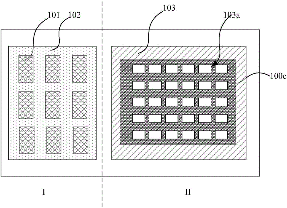
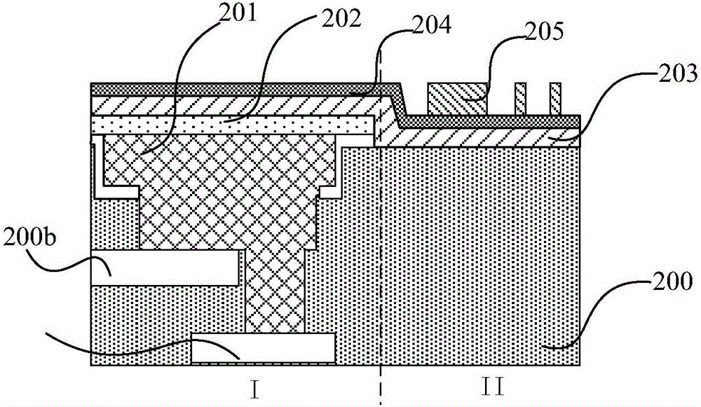
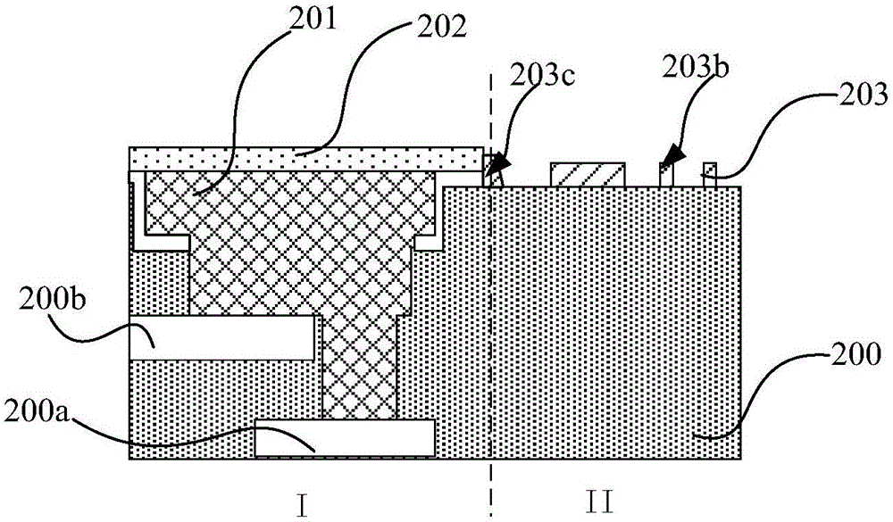
The invention provides a manufacturing method and layout structure of a back-illuminated sensor. In the layout structure, the range of a metal grid layer at least covers the boundary of a pixel layer of a protection layer near the pixel region, and thus in the manufacturing method, when the metal grid of the back-illuminated sensor is manufactured according to a new layout structure, the metal at the step of the protection layer and the pixel layer does not need to be etched, and thus the defects of metal residues can be avoided, the impact of the light transmittance in the pixel region can be avoided, and the performance of the back-illuminated image sensor chip which is finally prepared can be increased.

Description

technical field [0001] The invention relates to the technical field of manufacturing back-illuminated sensors, in particular to a manufacturing method and layout structure of a back-illuminated sensor. Background technique [0002] Light for backside illuminated (BSI) sensors enters the substrate from the backside of the substrate instead of the frontside, and because of reduced light reflections, BSI sensors are able to capture more image signals than frontside illuminated sensors. At present, the three-dimensional stacked back-illuminated sensor (UTS) integrates the logic operation chip and the pixel (photodiode) array chip in three dimensions through silicon vias (TSV: through Si Via). On the one hand, while maintaining the chip volume, it improves the sensor array. On the other hand, the metal interconnection between functional chips is greatly shortened, heat generation, power consumption, and delay are reduced, and chip performance is improved. [0003] In the three-d...

Claims


Application Information

Patent Timeline
Patent Type & Authority Applications(China)
IPC IPC(8): H01L27/146H01L27/02
CPCH01L27/0207H01L27/14601H01L27/14605H01L27/1464H01L27/14683
Inventor 占琼朱继锋
Owner WUHAN XINXIN SEMICON MFG CO LTD
Learn More