Wafer testing system and testing method thereof

A test system and test method technology, applied in the direction of single semiconductor device testing, etc., can solve the problems of inability to achieve adaptability and different instructions, and achieve the effects of improving test efficiency, reducing interference, and improving isolation.

Active Publication Date: 2017-05-31
珠海市中芯集成电路有限公司
View PDF15 Cites 6 Cited by
  • Summary
  • Abstract
  • Description
  • Claims
  • Application Information

AI Technical Summary

Problems solved by technology

However, with the diversification of chip products, some functional testers can no longer complete it alone. For example, some chips have random codes. After obtaining the random codes, the encryption algorithm can be run to calculate the instructions for chip operations, so different The instructions of IC chips are different, so the fixed test mode of the existing tester cannot achieve good adaptability

Method used


Image

  • Wafer testing system and testing method thereof
  • Wafer testing system and testing method thereof
  • Wafer testing system and testing method thereof

Examples


Embodiment Construction

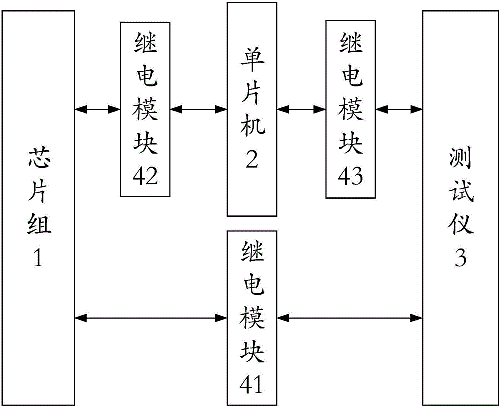
[0037] Wafer test system embodiment:

[0038] refer to figure 1 , figure 1 It is a system block diagram of the test system. There are multiple chips arranged on the wafer, and the multiple chips constitute the chipset 1 to be tested. The test system includes a tester 3, a first relay module 41, a single-chip microcomputer 2, and a second relay module 42 and the third relay module 43, the first relay module 41 is used to connect between the tester 3 and the chipset 1, the tester 3 can perform the first test on the chipset 1, and the first relay module 41 is used to receive The first on-off signal output by the tester 3 then realizes the on-off control of the first relay module 41 by the tester 3 .

[0039] The single-chip microcomputer 2 receives the starting signal of the tester 3, and the single-chip microcomputer 2 stores the key of the program and the chip, which is used to interact with the encrypted data of the corresponding chip. The single-chip microcomputer 2 perfo...


PUM


Abstract

The invention provides a wafer testing system and a testing method thereof. The wafer testing system comprises a testing instrument, a first relay module, a single-chip microcomputer, a second relay module and a third relay module, wherein the testing instrument is used for performing a first test on a wafer, the first relay module is connected between the testing instrument and the wafer and used for receiving a first on-off signal output by the testing instrument, the single-chip microcomputer receives a starting signal of the testing instrument and performs a second test on the wafer through an encryption algorithm, the second relay module is connected between the single-chip microcomputer and the wafer and used for receiving a second on-off signal output by the testing instrument, and the third relay module is connected between the testing instrument and the single-chip microcomputer and receives a third on-off signal output by the testing instrument. The wafer testing system has the advantages that the testing instrument and the single-chip microcomputer are used to perform different tests on the wafer respectively, switching can be performed by the relay modules, and testing efficiency can be increased greatly.

Description

technical field [0001] The invention relates to the field of wafer testing, in particular to a wafer testing system and a testing method of the testing system. Background technique [0002] Wafer refers to the silicon wafer used in the production of silicon semiconductor integrated circuits. Various circuit element structures can be processed on the wafer to become IC chips with specific electrical functions. After the wafer manufacturing is completed, wafer testing is a very important step of testing. Wafer testing is to test each IC chip on the wafer, and test its electrical characteristics by contacting the external contacts (pad) on the chip. See if it meets the factory standard. [0003] Wafer testing is generally carried out by a special tester, and when the tester is designed, only some of the more commonly used test items are packaged into the tester, and the logic functions of the verification chip are implemented using a fixed test mode. However, with the diversi...

Claims


Application Information

Patent Timeline
Patent Type & Authority Applications(China)
IPC IPC(8): G01R31/26
CPCG01R31/26
Inventor 吴俊袁志伟
Owner 珠海市中芯集成电路有限公司
Why Eureka
Try Eureka