C-axis crystal igzo thin film and preparation method thereof

A thin film and indium oxide film technology, which is applied in semiconductor/solid-state device manufacturing, coating, gaseous chemical plating, etc., can solve the problems of unfavorable large-scale application of C-axis crystal IGZO, so as to promote large-scale application and reduce production costs , the effect of good crystal quality

Active Publication Date: 2019-02-19
WUHAN CHINA STAR OPTOELECTRONICS TECH CO LTD
View PDF4 Cites 0 Cited by
  • Summary
  • Abstract
  • Description
  • Claims
  • Application Information

AI Technical Summary

Problems solved by technology

The research team of SEL (Semiconductor Energy Laboratory Co., Ltd) used magnetron sputtering to prepare C-axis crystalline IGZO thin films, but only the regions with a diameter of 1nm-3nm in the prepared C-axis crystalline IGZO thin films were in a crystalline state, which was absolutely impossible. Most of the regions are in the amorphous state, that is to say, in the C-axis crystalline IGZO thin film, only a very small region is C-axis crystalline IGZO, and the rest of the region is a-IGZO. Due to the small area of ​​the crystalline region, therefore It is not conducive to the large-scale application of C-axis crystalline IGZO

Method used


Image

  • C-axis crystal igzo thin film and preparation method thereof
  • C-axis crystal igzo thin film and preparation method thereof
  • C-axis crystal igzo thin film and preparation method thereof

Examples


Embodiment Construction

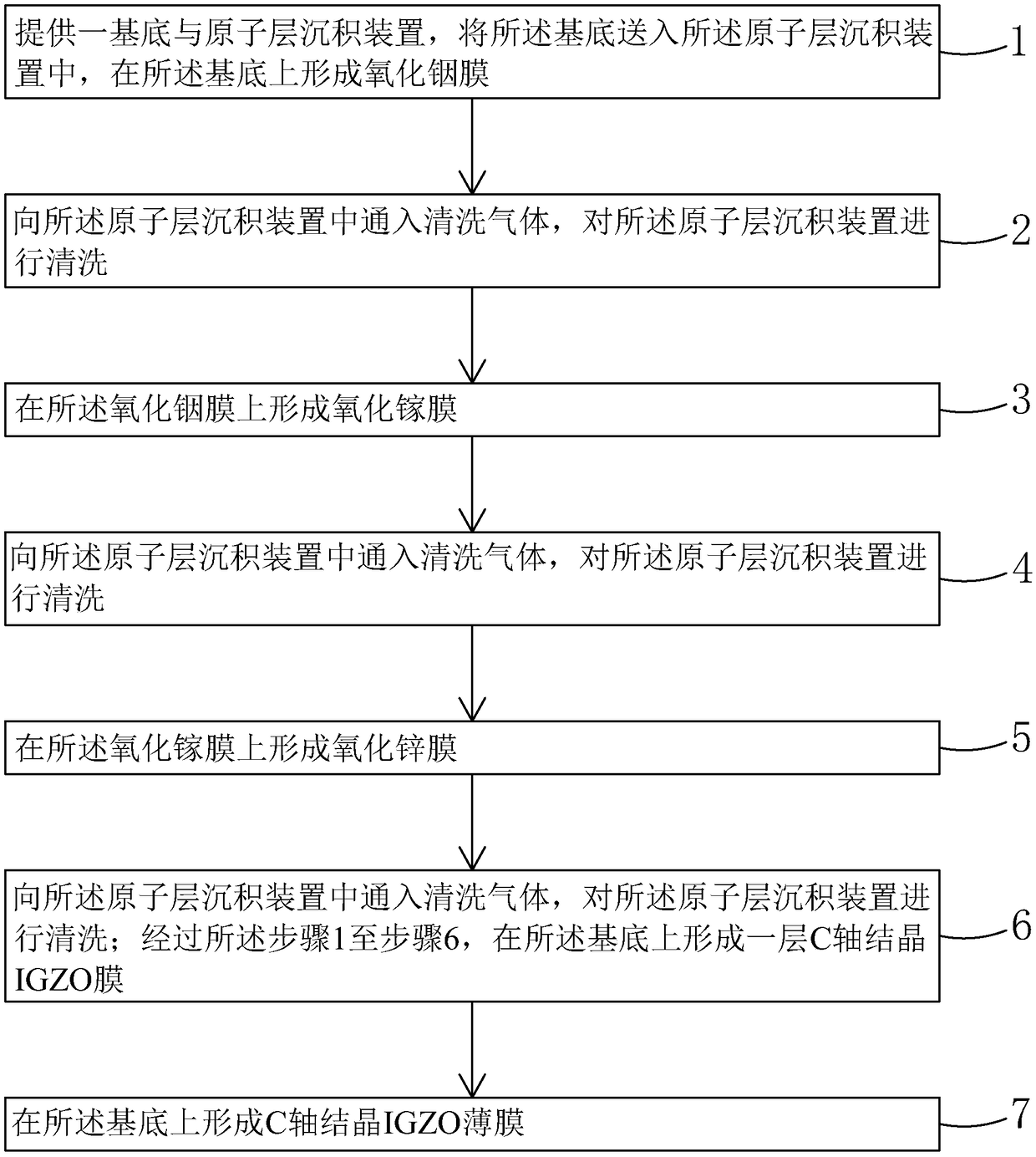
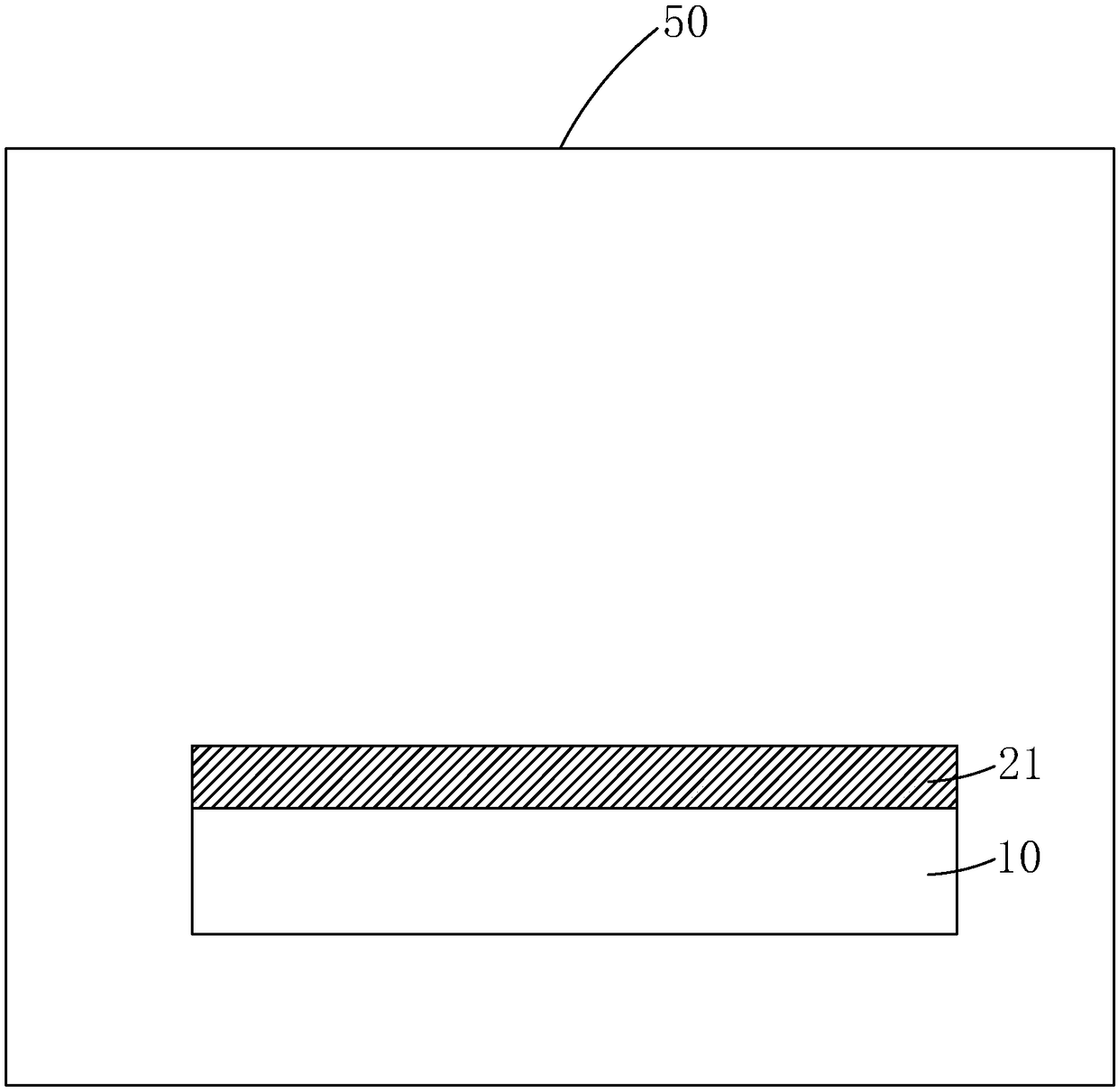
[0036] In order to further illustrate the technical means adopted by the present invention and its effects, the following describes in detail in conjunction with preferred embodiments of the present invention and accompanying drawings.

[0037] Atomic layer deposition (Atomic Layer Deposition, ALD) is a method of forming a deposited film by pulsating gaseous precursors alternately into the reactor to chemically adsorb and react on the deposition substrate. When the precursors reach the surface of the deposition substrate, they chemisorb and undergo surface reactions on the surface. The ALD reactor needs to be purged with an inert gas between precursor pulses. It can be seen that whether the precursor substances of the deposition reaction can be chemically adsorbed on the surface of the deposited material is the key to the realization of atomic layer deposition. The adsorption characteristics of gaseous substances on the surface of the matrix material can be seen that any gase...


PUM


Abstract

The invention provides a C-axis crystalline IGZO thin film and a preparation method thereof. The preparation method of the C-axis crystalline IGZO thin film of the present invention prepares the C-axis crystalline IGZO thin film by adopting the method of atomic layer deposition, which can precisely control the structure of the C-axis crystalline IGZO at the atomic level, and the crystallization of the obtained C-axis crystalline IGZO Good quality, less oxygen defects, can improve the stability of TFT; and because the area of ​​the crystalline region in the C-axis crystalline IGZO film prepared by the present invention is relatively large, reaching hundreds of microns to millimeters, it can promote C-axis crystallization Large-scale application of IGZO; at the same time, the present invention utilizes optimized process conditions to prepare C-axis crystalline IGZO thin films, which can improve production yield and reduce production costs. The C-axis crystalline IGZO thin film of the present invention has good crystallization quality of the C-axis crystalline IGZO, less oxygen defects, can improve the stability of TFT, and meanwhile has a larger crystallization area, which is beneficial to the large-scale application of the C-axis crystalline IGZO.

Description

technical field [0001] The invention relates to the field of display technology, in particular to a C-axis crystalline IGZO thin film and a preparation method thereof. Background technique [0002] Thin Film Transistor (TFT) is the main driving element in current Liquid Crystal Display (LCD) and Active Matrix Organic Light-Emitting Diode (AMOLED). It is related to the development direction of high-performance flat panel display devices. [0003] With the rise of terminal applications such as smartphones and flat panel displays, the requirement for high-definition panels above 250PPI (Pixels Per Inch, the number of pixels per inch) has gradually become a matching trend, which has also prompted more panel manufacturers to invest in high-definition The production of Low Temperature Polysilicon (LTPS) thin film transistors is expanding. However, due to the high process complexity of the low temperature polysilicon TFT (LTPS TFT) production line, and the yield rate is also a big...

Claims


Application Information

Patent Timeline
Patent Type & Authority Patents(China)
IPC IPC(8): C23C16/40C23C16/455
CPCC23C16/40C23C16/407C23C16/45529C23C16/45531H01L21/02554H01L21/02661H01L21/02609H01L21/02565H01L21/0262C23C16/45534C23C16/4408H01L29/7869C23C16/45544H01L27/1262H01L27/1225
Inventor 王选芸
Owner WUHAN CHINA STAR OPTOELECTRONICS TECH CO LTD
Why Eureka
Try Eureka