
A zinc oxide nanorod/black silicon heterojunction nanophotodetector and its preparation method

A zinc oxide nanorod, photodetector technology, applied in the field of photodetectors, can solve the problems of small photosensitive area, insufficient absorption of incident light, low sensitivity, etc., to increase the photosensitive area, overcome large transmission loss, and improve sensitivity Effect

Inactive Publication Date: 2018-01-19
HEFEI UNIV OF TECH
View PDF6 Cites 0 Cited by
  • Summary
  • Abstract
  • Description
  • Claims
  • Application Information

AI Technical Summary

Problems solved by technology

This makes zinc oxide photodetectors have the problems of small photosensitive area, insufficient absorption of incident light and low sensitivity.

Method used


Image

  • A zinc oxide nanorod/black silicon heterojunction nanophotodetector and its preparation method
  • A zinc oxide nanorod/black silicon heterojunction nanophotodetector and its preparation method
  • A zinc oxide nanorod/black silicon heterojunction nanophotodetector and its preparation method

Examples


Embodiment 1

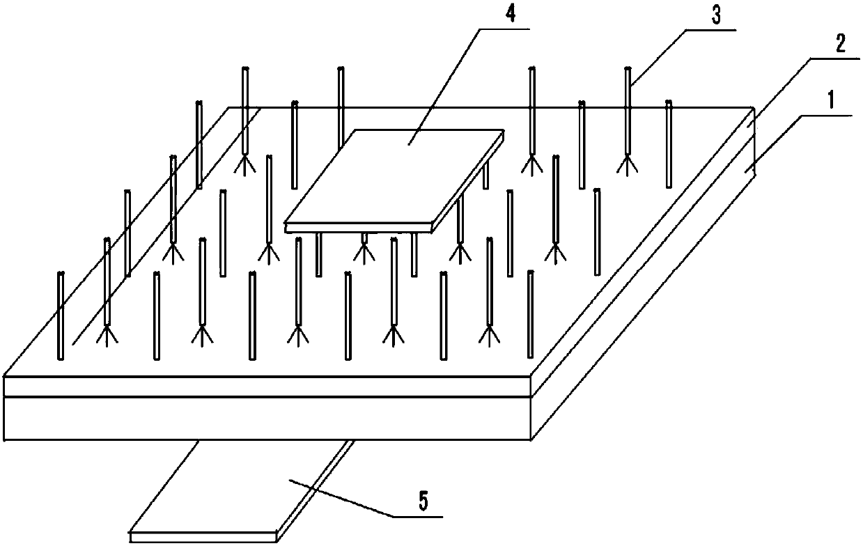
[0033] like figure 1 As shown, the zinc oxide nanorod / black silicon heterojunction nanophotodetector of the present embodiment uses a p-type silicon chip as the substrate 1, and a black silicon layer 2 is formed on the upper surface of the substrate 1. A zinc oxide nanorod array layer 3 is formed on the silicon layer 2; a top electrode 4 is arranged on the zinc oxide nanorod array layer 3; a bottom electrode 5 is arranged on the lower surface of the substrate 1. Wherein, the zinc oxide nanorods constituting the zinc oxide nanorod array layer 3 grow vertically to the black silicon layer. The surface of the p-type silicon wafer is formed with a pyramid structure. Both the top electrode 4 and the bottom electrode 5 are silver electrodes formed by applying silver paste.

[0034] The nano photodetector of the present embodiment is prepared according to the following steps:

[0035] 1. Use acetone, alcohol and pure water to ultrasonically clean the p-type silicon wafer, and then ...

Embodiment 2

[0049] The structure of the zinc oxide nanorod / black silicon heterojunction nanophotodetector of this embodiment is the same as that of Example 1, and the preparation method is basically the same, the only difference being that the growth solution in step 5 is: 0.2g zinc nitrate hexahydrate and 0.21g urotropine was dissolved in 30mL water.

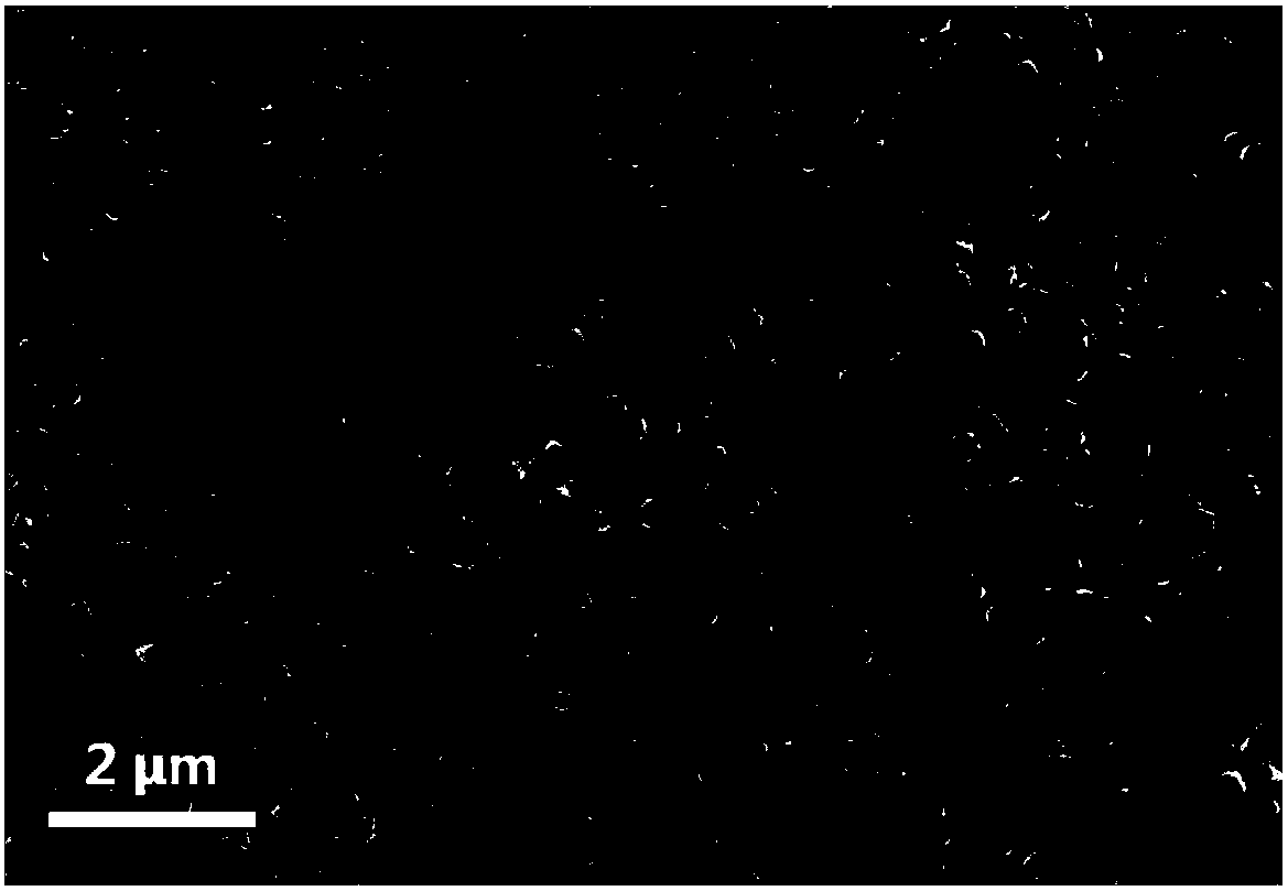
[0050] The field emission scanning electron microscope picture (top view) of the zinc oxide nanorod array grown on the black silicon layer of the present embodiment is as Figure 6 As shown, it can be seen from the figure that when the concentration of zinc nitrate hexahydrate is relatively small, the diameter of the grown zinc oxide nanorods is relatively smaller and denser at the same time.

Embodiment 3

[0052] The structure of the zinc oxide nanorod / black silicon heterojunction nanophotodetector of this embodiment is the same as that of Example 1, and the preparation method is basically the same, the only difference being that the growth solution in step 5 is: 0.6g zinc nitrate hexahydrate and 0.21g urotropine was dissolved in 30mL water.

[0053] The field emission scanning electron microscope picture (top view) of the zinc oxide nanorod array grown on the black silicon layer of the present embodiment is as Figure 7 It can be seen from the figure that when the concentration of zinc nitrate hexahydrate is relatively high, the diameter of the grown zinc oxide nanorods is relatively larger and more sparse.


PUM


Abstract

The invention discloses a zinc oxide nanorod / black silicon heterojunction nanometer photoelectric detector and a fabrication method thereof. The zinc oxide nanorod / black silicon heterojunction nanometer photoelectric detector is characterized in that a p-type silicon wafer is used as a substrate, a black silicon layer is formed on an upper surface of the substrate, a zinc oxide nanorod array layer is formed on the black silicon layer, a top electrode is formed on the zinc oxide nanorod array layer, and a bottom electrode is arranged on a lower surface of the substrate. In the nanometer photoelectric detector, the zinc oxide nanorod array is used as a main light sensitive layer, nanorods are uniformly and densely arranged, the nanometer photoelectric detector has relatively large specific area, so that the light sensitive area of the nanometer photoelectric detector is remarkably expanded, the number of photon-generated carriers is substantially increased, and the sensitivity of a nanometer photovoltaic device is improved.

Description

technical field [0001] The invention relates to a photodetector, more specifically to a zinc oxide nanorod / black silicon heterojunction nanophotodetector and a preparation method thereof. Background technique [0002] Photodetection devices can convert the sensed light signal into electrical signal, which has important military value and broad civilian market. The structural layers of a photodetector device are an insulating substrate, a photosensitive layer, and an electrode from bottom to top. Nanophotodetectors are photodetectors that use nanomaterials as the photosensitive layer, which has the characteristics of easy integration, low power consumption, and low cost. More importantly, nano photodetectors have higher sensitivity and response speed than thin film photodetectors of the same material. Zinc oxide is a group II-VI semiconductor material widely studied in recent years. It has a bandgap at room temperature of ~3.37eV, an exciton binding energy of ~60meV, and is...

Claims


Application Information

Patent Timeline
Patent Type & Authority Patents(China)
IPC IPC(8): H01L31/101H01L31/18H01L31/0352H01L31/0296H01L31/0236
CPCH01L31/0236H01L31/0296H01L31/0352H01L31/101H01L31/18Y02E10/50Y02P70/50
Inventor 王莉任治飞何淑娟李晶晶于永强吴春艳罗林保
Owner HEFEI UNIV OF TECH
Learn More