


Quick Research
Generate reliable direction feasibility study reports for your R&D in just a few steps.

Technical Q&A
Discover and master advanced knowledge NOW. Basics, ideas, possibilities, all at once.

Find Solutions
As an expert in R&D theories, this can generate solutions to your technical problems instantly.

Evaluate Feasibility
Analyze your overall solution with one click, know your potential R&D risks in advance.

Monitor Landscape
Get weekly tech updates, stay abreast of the latest tech innovations and key insights.
Pixel structure, display panel and display device
A pixel structure and sub-pixel technology, applied in the direction of instruments, nonlinear optics, optics, etc., can solve the problem of poor display of horizontal, vertical or twill lines in solid color screens, poor display of horizontal and vertical twill lines, high density of main PS, etc. problems, to achieve the effect of reducing production yield, consistent display effect, and increasing cost
- Summary
- Abstract
- Description
- Claims
- Application Information
AI Technical Summary
Problems solved by technology
Method used
Image


Examples
Embodiment 1
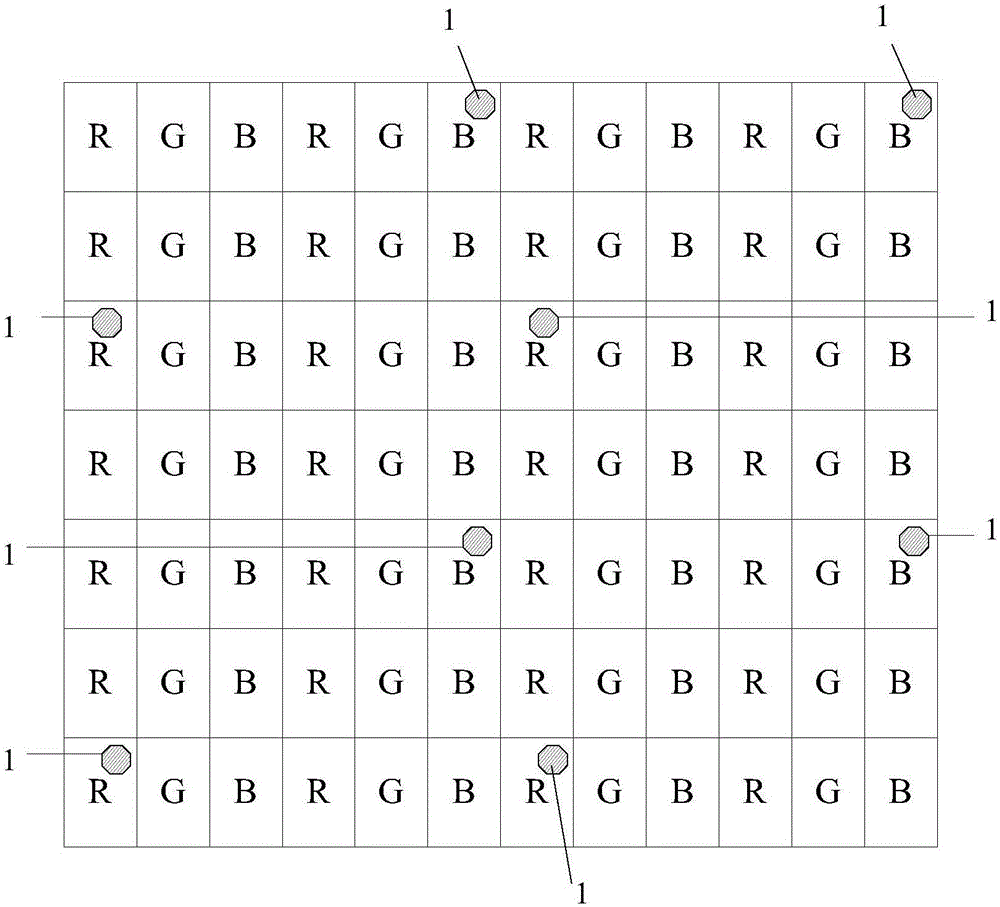
[0035] Embodiment one, such as image 3As shown, R, G, and B in the figure respectively represent red, green, and blue sub-pixel regions, and the main spacer 1 is disposed in the red sub-pixel region and the blue sub-pixel region. Set N main spacers in the pixel structure, and set the main spacers in the red sub-pixel area and the blue sub-pixel area in equal proportions, that is, set N / 2 main spacers in the red sub-pixel area and the blue sub-pixel area respectively. Spacers, compared to only setting main spacers in sub-pixel areas of one color, can reduce the density of main spacers in sub-pixel areas of one color, thereby reducing the occurrence of horizontal and vertical lines in solid-color screens Or the risk of poor twill display, and the density of the main spacer in the red sub-pixel area and the blue sub-pixel area is consistent, and the corresponding display effect of the solid color screen of the corresponding color is consistent, which further improves the display...
Embodiment 2
[0036] Embodiment two, such as Figure 4 As shown, R, G, and B in the figure respectively represent red, green, and blue sub-pixel regions, and the main spacer 1 is disposed in the blue sub-pixel region and the green sub-pixel region. Set N main spacers in the pixel structure, and set the main spacers in the blue sub-pixel area and the green sub-pixel area in equal proportions, that is, set N / 2 main spacers in the blue sub-pixel area and the green sub-pixel area respectively. Spacers, compared to only setting main spacers in sub-pixel areas of one color, can reduce the density of main spacers in sub-pixel areas of one color, thereby reducing the occurrence of horizontal and vertical lines in solid-color screens Or the risk of poor twill display, and the density of the main spacer in the blue sub-pixel area and the green sub-pixel area is consistent, and the corresponding display effect of the solid color screen of the corresponding color is consistent, which further improves t...
Embodiment 3
[0037] Embodiment three, such as Figure 5 As shown, R, G, and B in the figure respectively represent red, green, and blue sub-pixel regions, and the main spacer 1 is disposed in the red sub-pixel region and the green sub-pixel region. Set N main spacers in the pixel structure, and set the main spacers in the red sub-pixel area and the green sub-pixel area in equal proportions, that is, set N / 2 main spacers in the red sub-pixel area and the green sub-pixel area respectively Compared with only setting the main spacer in the sub-pixel area of one color, the density of the main spacer in the sub-pixel area of one color can be reduced, thereby reducing the occurrence of horizontal, vertical or diagonal lines in the solid-color screen The risk of poor display, and the density of the main spacer in the red sub-pixel area and the green sub-pixel area is consistent, and the corresponding display effect of the solid color screen of the corresponding color is consistent, which furth...
PUM
 Abstract
Description
Claims
Application Information
 - R&D Engineer
- R&D Manager
- IP Professional
- Industry Leading Data Capabilities
- Powerful AI technology
- Patent DNA Extraction
Browse by: Latest US Patents, China's latest patents, Technical Efficacy Thesaurus, Application Domain, Technology Topic, Popular Technical Reports.
© 2024 PatSnap. All rights reserved.Legal|Privacy policy|Modern Slavery Act Transparency Statement|Sitemap|About US| Contact US: help@patsnap.com