High-linearity sine-wave generator with multiplying clock multiple following
A sine wave generator, high linearity technology, applied in electrical components and other directions, can solve problems such as large capacitance value, large area, and inability to achieve frequency stability, and achieve the effect of improving linearity, design and implementation.
- Summary
- Abstract
- Description
- Claims
- Application Information
AI Technical Summary
Problems solved by technology
Method used
Image
Examples
Embodiment 1
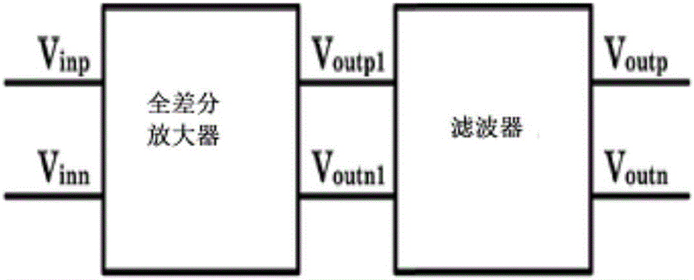
[0024] see figure 1 , figure 2 and image 3 , a high-linearity sine wave generator followed by clock multiples, including a reference voltage input terminal Vref, a ground terminal, a fully differential amplifier, and a plurality of series-connected voltage-dividing resistors. The voltage-dividing resistors include the zeroth resistor R 0 , the first resistor R 1 , the second resistance R 2 ...the N+2th resistor Rn+2, the zeroth resistor R 0 One end of Rn is connected to the reference voltage input end, the N+2th resistor Rn+2 is connected to the ground end, and a first voltage output point V is respectively set between multiple voltage dividing resistors 1 , the second voltage output point V2...the N+1th voltage output point V N+1 . Among them, the first voltage output point is set at the zero resistance R 0 with the first resistor R 1 Between, and so on, the setting position of N+1 voltage output points is between two voltage divider resistors.
[0025] Such as f...
Embodiment 2
[0044] see Figure 4 , a clock signal with a stable frequency is input from the crystal oscillator to a high-linearity sine wave generator followed by a multiplier of the clock. The high-linearity sine wave generator followed by the clock multiple produces a differential output clock to follow the stable frequency sine wave signal to the substrate of the sensor, and the positive terminal outputs V outp Connect the upper substrate V of the sensor st , the negative terminal outputs V outn Connect the lower substrate V of the sensor sb [The connection can also be reversed to output V for the positive terminal. outp Connect the lower substrate V of the sensor sb , the negative terminal outputs V outn Connect the upper substrate V of the sensor st 】. The substrate of the sensor V ctr Connect the negative terminal input of the front-end amplifier, connect the feedback capacitor C f One end, connected to the feedback resistor R f one end. The positive terminal input of the...
PUM
 Abstract
Description
Claims
Application Information
 - R&D
- Intellectual Property
- Life Sciences
- Materials
- Tech Scout
- Unparalleled Data Quality
- Higher Quality Content
- 60% Fewer Hallucinations
Browse by: Latest US Patents, China's latest patents, Technical Efficacy Thesaurus, Application Domain, Technology Topic, Popular Technical Reports.
© 2025 PatSnap. All rights reserved.Legal|Privacy policy|Modern Slavery Act Transparency Statement|Sitemap|About US| Contact US: help@patsnap.com


