
High-beam-quality large-scale VCSEL in-phase coupled array

A coupling array and high-beam technology, which is applied to lasers, laser components, semiconductor lasers, etc., can solve the problems of high cost and achieve the effects of low cost, high beam quality, and easy promotion and application

Inactive Publication Date: 2017-05-10
BEIJING UNIV OF TECH
View PDF4 Cites 8 Cited by
  • Summary
  • Abstract
  • Description
  • Claims
  • Application Information

AI Technical Summary

Problems solved by technology

Although the in-phase coupling VCSEL array can be realized by using the cavity-induced anti-waveguide structure, the cavity-induced anti-waveguide structure requires complex preparation processes such as secondary epitaxy, and the cost is very expensive.

Method used


Image

  • High-beam-quality large-scale VCSEL in-phase coupled array
  • High-beam-quality large-scale VCSEL in-phase coupled array
  • High-beam-quality large-scale VCSEL in-phase coupled array

Examples


Embodiment Construction

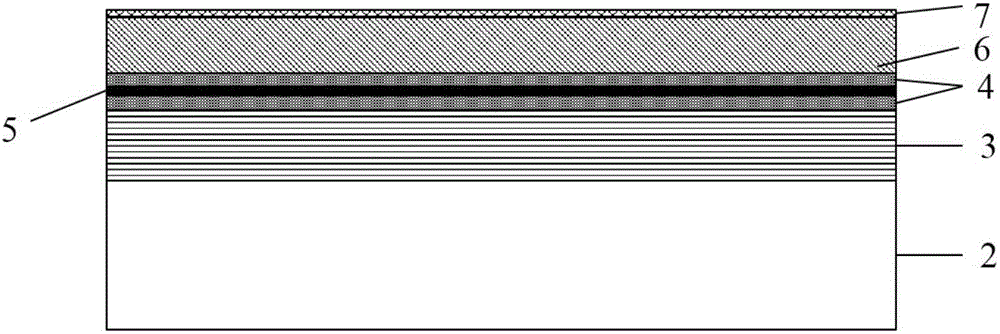
[0028] Combine below Figure 4-Figure 12 The specific implementation methods of the preparation method of large-scale VCSEL in-phase coupling array with high beam quality are introduced respectively;

[0029] Step 1. Using metal-organic chemical vapor deposition (MOCVD) to sequentially epitaxially grow thirty-four pairs of n-Al on N-GaAs (0.12-0.9) GaAs and n-Al 0.9 GaAs forms the DBR mirror, Al (0.12-0.9) GaAs / Al 0.9 GaAs lower confinement layer, three pairs of Al 0.3 GaAs / GaAs quantum well structure active region, Al 0.9 GaAs / Al (0.12-0.9) GaAs upper confinement layer, 22.5 to p-Al 0.12 GaAs and p-Al (0.9-0.12) GaAs forms the DBR mirror, p-Al 0.12 GaAs and p-GaAs heavily doped contact layers;

[0030] Step 2, using plasma-enhanced chemical vapor deposition (PECVD) to grow a layer of 3.2 μm silicon dioxide on the surface of the epitaxial wafer obtained above;

[0031] Step 3. Use reverse glue to do photolithography and sputtering process to sputter a layer of silico...


PUM

PropertyMeasurementUnit
Thicknessaaaaaaaaaa
Widthaaaaaaaaaa
Widthaaaaaaaaaa

Abstract

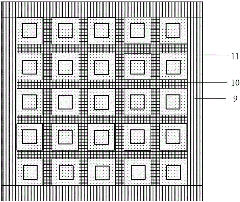
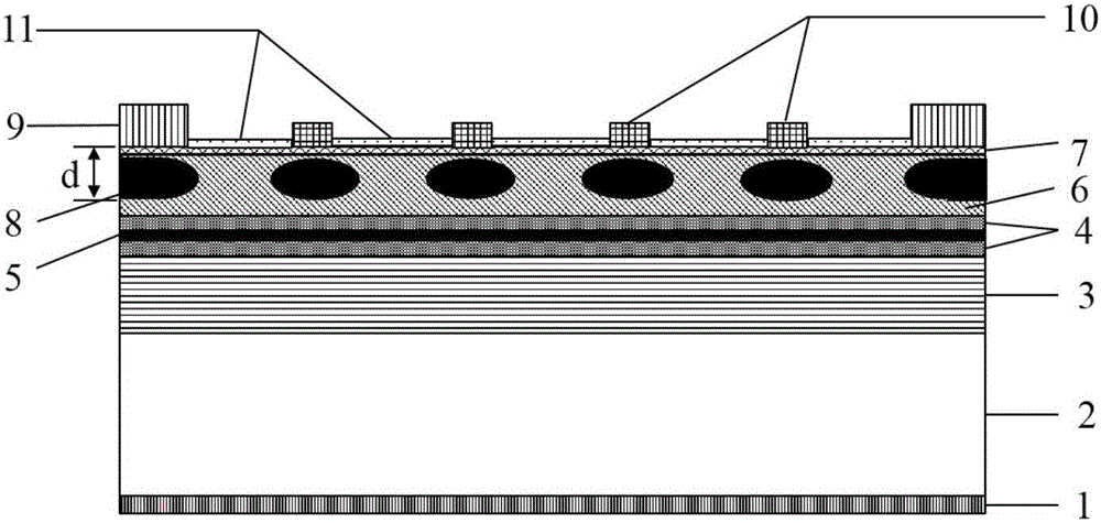
The invention discloses a high-beam-quality large-scale VCSEL in-phase coupled array and belongs to the field of semiconductor laser unit technology. The high-beam-quality large-scale VCSEL in-phase coupled array is provided with grid electrodes. A proton injection method is adopted to realize electrical isolation between light-out units. When a device operates, the effective refractive index of each light outlet region is lower than the effective refractive index of each interval region, and a special anti-waveguide structure is formed. The grid electrodes in the interval regions further enlarge anti-waveguide refractive index steps, so that in-phase coupling difficulty is lowered. By properly adjusting proton injection depth d and unit spacing, the array satisfies in-phase laser emission conditions, and the in-phase coupled array can be realized. By reasonably designing the array unit spacing and the proton injection depth d, in-phase laser output can be obtained, the beam quality of the array is improved, and the array can be applied to the fields of free space optical interconnection, laser radar, laser printing, optical fiber communication, optical pumping, etc.

Description

technical field [0001] The invention belongs to the technical field of semiconductor lasers, and in particular relates to a large-scale VCSEL in-phase coupling array with simple process and low cost and high beam quality. Background technique [0002] High-beam quality and high-power vertical-cavity surface-emitting laser arrays have a wide range of applications in pumping, laser printing, free-space optical communications, and high-density optical storage. The in-phase coupling array can not only achieve single-mode lasing, but also can obtain high beam quality near the diffraction limit, and the far-field center light intensity has a maximum value, which has greater advantages in applications such as fiber coupling. However, when the scale of the array increases to a certain extent, it is necessary to use grid electrodes to achieve uniform injection of current. However, the introduction of electrodes makes the array often in anti-phase lasing, and the center of the far fi...

Claims


Application Information

Patent Timeline
IPC IPC(8): H01S5/183H01S5/323H01S5/42
CPCH01S5/183H01S5/323H01S5/423
Inventor 徐晨潘冠中荀孟王秋华解意洋
Owner BEIJING UNIV OF TECH
Learn More