
Patsnap Eureka
For R&D, Patsnap Eureka makes reading and utilizing patents & technical documents easy.
Patsnap Eureka AIR
Designed for self-driven R&D workflows. Generate viable solutions, solve complex R&D challenges, empower your innovation with AI.

Patsnap Eureka Materials
Designed for material experts only. Revolutionize your material R&D, from search, analyze, to developing new materials.

TechResearch
Generate reliable direction feasibility study reports for your R&D in just a few steps.

TechSeek
Discover and master advanced knowledge NOW. Basics, ideas, possibilities, all at once.

TechMind
As an expert in R&D Theories, TechMind can generates customized viable solutions instantly.

TechRisk
Analyze your overall solution with one click, know your potential R&D risks in advance.

TechMonitor
Get weekly tech updates, stay abreast of the latest tech innovations and key insights.
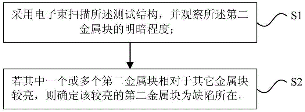
Testing structure and testing method of semiconductor
A technology for testing structures and semiconductors, which is used in semiconductor/solid-state device testing/measurement, semiconductor devices, and semiconductor/solid-state device components, etc. It can solve the problems of long periods and inability to monitor through-hole metal conductive pillars in real time, and achieve a simple structure. Effect
- Summary
- Abstract
- Description
- Claims
- Application Information
AI Technical Summary
Problems solved by technology
Method used
Image


Examples
Embodiment 1
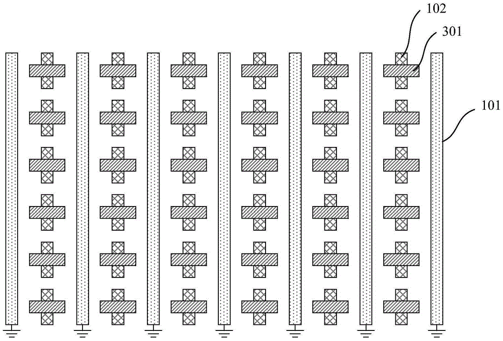
[0047] The present invention provides a semiconductor test structure, please refer to figure 1 , shown as a cross-sectional view of the semiconductor test structure, including:
[0048] The first metal layer 100; the first metal layer 100 includes at least two ground metal lines 101 arranged in parallel, and at least two rectangular first metal blocks 102 are formed between two adjacent ground metal lines 101; A metal block 102 is arranged in the same direction as the ground metal wire 101;
[0049] The second metal layer 200; the second metal layer 200 includes a plurality of metal conductive pillars 201 corresponding to the first metal block 102, and the metal conductive pillars 201 are connected to the top of the first metal block 102;
[0050] The third metal layer 300; the third metal layer 300 includes a plurality of rectangular second metal blocks 301 corresponding to the metal conductive columns, the second metal blocks 301 are connected to the top of the metal conduc...
Embodiment 2
[0066] This embodiment adopts basically the same technical solution as Embodiment 1, except that the semiconductor test structure of Embodiment 1 includes only one block, while the semiconductor test structure of this embodiment includes at least two blocks.
[0067] see Figure 4 , shown as a top view of the semiconductor test structure in this embodiment, as shown in the figure, the semiconductor test structure includes at least two blocks, such as the first block I, the second block II, and the third block III ,……. Each block is composed of the first metal layer 100, the second metal layer 200, and the third metal layer 300 as described in Embodiment 1, that is, the first metal layer 100 includes at least two ground metal lines arranged in parallel 101, at least two rectangular first metal blocks 102 are formed between two adjacent ground metal lines 101; the arrangement direction of the first metal blocks 102 and the ground metal lines 101 is the same; the second metal la...
PUM
 Abstract
Description
Claims
Application Information
 - R&D Engineer
- R&D Manager
- IP Professional
- Industry Leading Data Capabilities
- Powerful AI technology
- Patent DNA Extraction
Browse by: Latest US Patents, China's latest patents, Technical Efficacy Thesaurus, Application Domain, Technology Topic, Popular Technical Reports.
© 2024 PatSnap. All rights reserved.Legal|Privacy policy|Modern Slavery Act Transparency Statement|Sitemap|About US| Contact US: help@patsnap.com