Touch display panel and sensing and driving method thereof
A technology for touch display panels and sensing electrodes, which is applied in the directions of instruments, calculations, and electrical digital data processing, etc., which can solve the problems of increased module thickness, more bonding work, and violation of the ultra-thin trend, and achieve a reduction in overall thickness , Reduce the effect of lamination
- Summary
- Abstract
- Description
- Claims
- Application Information
AI Technical Summary
Problems solved by technology
Method used
Image
Examples
no. 1 example
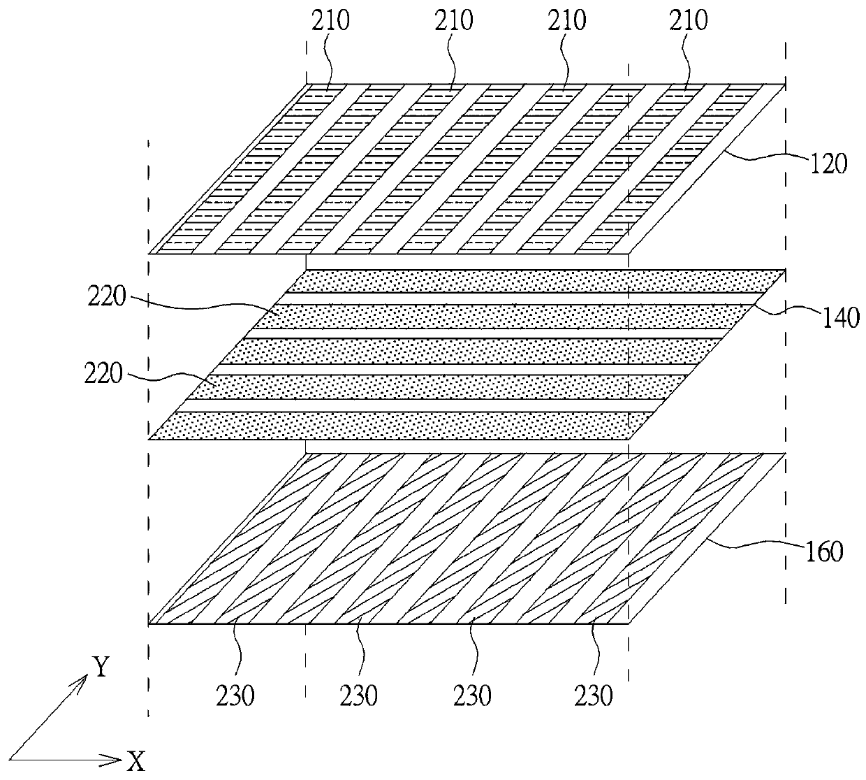
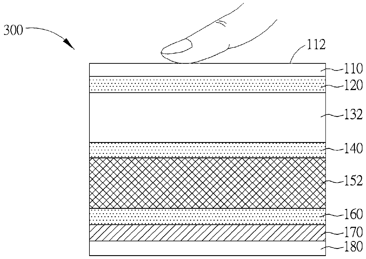
[0066] Please refer to image 3 , image 3 It is a stacked diagram of the touch display panel 300 having the electrode layer 120 , the electrode layer 140 and the electrode layer 160 according to the first embodiment of the present invention. The touch display panel 300 can be applied to a display panel in which the common electrode layer and the array layer are closely adjacent to each other, such as horizontal electric field switching (In Plane Switching; IPS). The touch display panel 300 includes an upper substrate 110 , an electrode layer 120 , a dielectric layer 130 , an electrode layer 140 , a dielectric layer 150 , an electrode layer 160 , an array layer 170 and a lower substrate 180 from top to bottom. Wherein, the dielectric layer 130 can be a color filter layer 132 , and the dielectric layer 150 can be a liquid crystal gap (cell gap) layer 152 . The structure of the three electrode layers 120, 140 and 160 of the touch display panel 300 can be as described above (eg...
no. 2 example
[0068] Please refer to Figure 4 , Figure 4 It is a stacked diagram of a touch display panel 400 with three electrode layers 120 , 140 and 160 according to the second embodiment of the present invention. The touch display panel 400 includes an electrode layer 120 , a dielectric layer 130 , an electrode layer 140 , a dielectric layer 150 , an electrode layer 160 , an array layer 170 and a substrate 180 from top to bottom. Wherein, the dielectric layer 130 can be the upper substrate 110 and is interposed between the electrode layer 120 and the electrode layer 140 . The dielectric layer 150 may include a filter layer 132 and a liquid crystal layer 152 between the electrode layer 140 and the electrode layer 110 . In addition, the structures of the three electrode layers 120, 140 and 160 of the touch display panel 300 can be as described above (eg figure 2 ).
no. 3 example
[0070] Please refer to Figure 5 , Figure 5 It is a stacked diagram of a touch display panel 500 having three electrode layers 120 , 140 and 160 according to the third embodiment of the present invention. The touch display panel 500 can be applied to a display panel in which the common electrode layer and the array layer of horizontal electric field switching (IPS) are adjacent. The touch display device 500 includes an electrode layer 120 , a dielectric layer 130 , an electrode layer 140 , a dielectric layer 150 , an electrode layer 160 , an array layer 170 and a lower substrate 180 from top to bottom. Wherein, the dielectric layer 130 can be an insulating layer (insulator) 122 , and the dielectric layer 150 can be the upper substrate 110 , the filter layer 132 and the liquid crystal layer 152 . In addition, the structure of the three electrode layers 120, 140 and 160 of the touch display panel 300 can be as follows figure 2 mentioned.
[0071] The detailed operation of ...
PUM
 Abstract
Description
Claims
Application Information
 - R&D Engineer
- R&D Manager
- IP Professional
- Industry Leading Data Capabilities
- Powerful AI technology
- Patent DNA Extraction
Browse by: Latest US Patents, China's latest patents, Technical Efficacy Thesaurus, Application Domain, Technology Topic, Popular Technical Reports.
© 2024 PatSnap. All rights reserved.Legal|Privacy policy|Modern Slavery Act Transparency Statement|Sitemap|About US| Contact US: help@patsnap.com


