Method for characterization of graphene epitaxially grown on SiC based on Ag-particle Raman enhancement effect
An enhancement effect, graphene technology, applied in the field of microelectronic materials, can solve the problems of sample contamination, difficulty in sample preparation, inability to directly characterize the degree of hydrogen insertion, etc., to achieve the effect of strong operability and simple method.
- Summary
- Abstract
- Description
- Claims
- Application Information
AI Technical Summary
Problems solved by technology
Method used
Image
Examples
Embodiment 1
[0043] The Raman spectrometer used in this example is Horiba HR800, and the laser excitation wavelength is 532nm. SiC substrate is used, the conductivity type is semi-insulating or N-type, the substrate surface is biased forward or 4°, 8°, the diameter is 2-6 inches, and the thickness is 300μm-400μm.
[0044] A method for characterizing the Raman enhancement effect of Ag particles based on SiC epitaxial graphene, comprising the following steps:
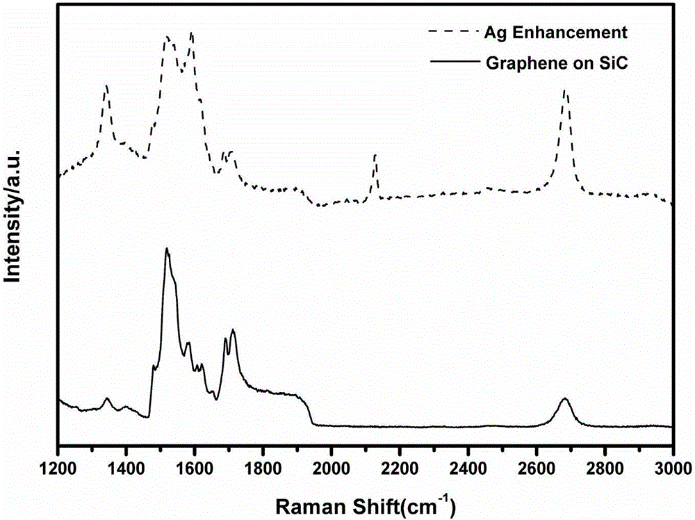
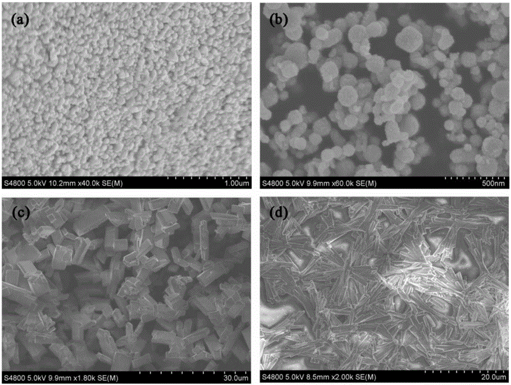
[0045] (1) Prepare 0.5mol / L AgNO 3 Solution; the ratio of the amount of substance is 4:1 to prepare the NaBH of 0.125mol / L 4 solution, add an appropriate amount of NaOH; under magnetic stirring, control 2mL / min to NaBH 4 The solution was added dropwise to AgNO 3 In the solution, the reaction temperature is controlled at 40-50° C. until the reaction is completed; the reaction product is centrifuged at a high speed of 9000 r / min, and washed with deionized water and ethanol to obtain Ag particles. figure 1 In the obtained Ag particle...
Embodiment 2
[0049] According to the characterization method identical with embodiment 1, its difference is:
[0050] Prepare 0.01mol / L AgNO 3 Solution, choose sodium citrate as the reducing agent, control the speed of 1mL / min to drop the reducing agent on the AgNO 3 In the solution, Ag sol is prepared, the Ag sol is dropped on the quasi-free state graphene wafer, heated to volatilize the liquid, and the quasi-free state graphene wafer with Ag particles deposited on the surface is obtained. The morphology of Ag particles is shown in image 3 In (c), (d) shown.
[0051] Graphene grown in situ on a SiC (0001) substrate was passed through H at 1000 °C 2 5h, carry out Raman characterization on it, get as follows figure 2 The Raman enhanced spectrum shown, and 2130cm -1 The proportion of the area with obvious Si-H bond response in the vicinity reaches 50%, that is, the buffer layer is removed in a large range.
Embodiment 3
[0053] According to the characterization method identical with embodiment 1, its difference is:
[0054] In step (1), first weigh 1 g of PVP as a surfactant, place it in deionized water, and fully dissolve it under ultrasonic conditions; then use this solution to prepare AgNO3 solution.
[0055] Graphene grown in situ on a SiC (0001) substrate was passed through H at 1500 °C 2 1h, using the same characterization method, the proportion of the area with Si-H bond response in the Raman spectrum reaches 100%, that is, the buffer layer is basically removed.
PUM
| Property | Measurement | Unit |
|---|---|---|
| diameter | aaaaa | aaaaa |
| length | aaaaa | aaaaa |
| width | aaaaa | aaaaa |
Abstract
Description
Claims
Application Information
 - R&D
- Intellectual Property
- Life Sciences
- Materials
- Tech Scout
- Unparalleled Data Quality
- Higher Quality Content
- 60% Fewer Hallucinations
Browse by: Latest US Patents, China's latest patents, Technical Efficacy Thesaurus, Application Domain, Technology Topic, Popular Technical Reports.
© 2025 PatSnap. All rights reserved.Legal|Privacy policy|Modern Slavery Act Transparency Statement|Sitemap|About US| Contact US: help@patsnap.com


