optical imaging system
An optical imaging system and imaging surface technology, applied in optics, optical components, instruments, etc., can solve problems such as inability to meet photography requirements
- Summary
- Abstract
- Description
- Claims
- Application Information
AI Technical Summary
Problems solved by technology
Method used
Image
Examples
no. 1 example
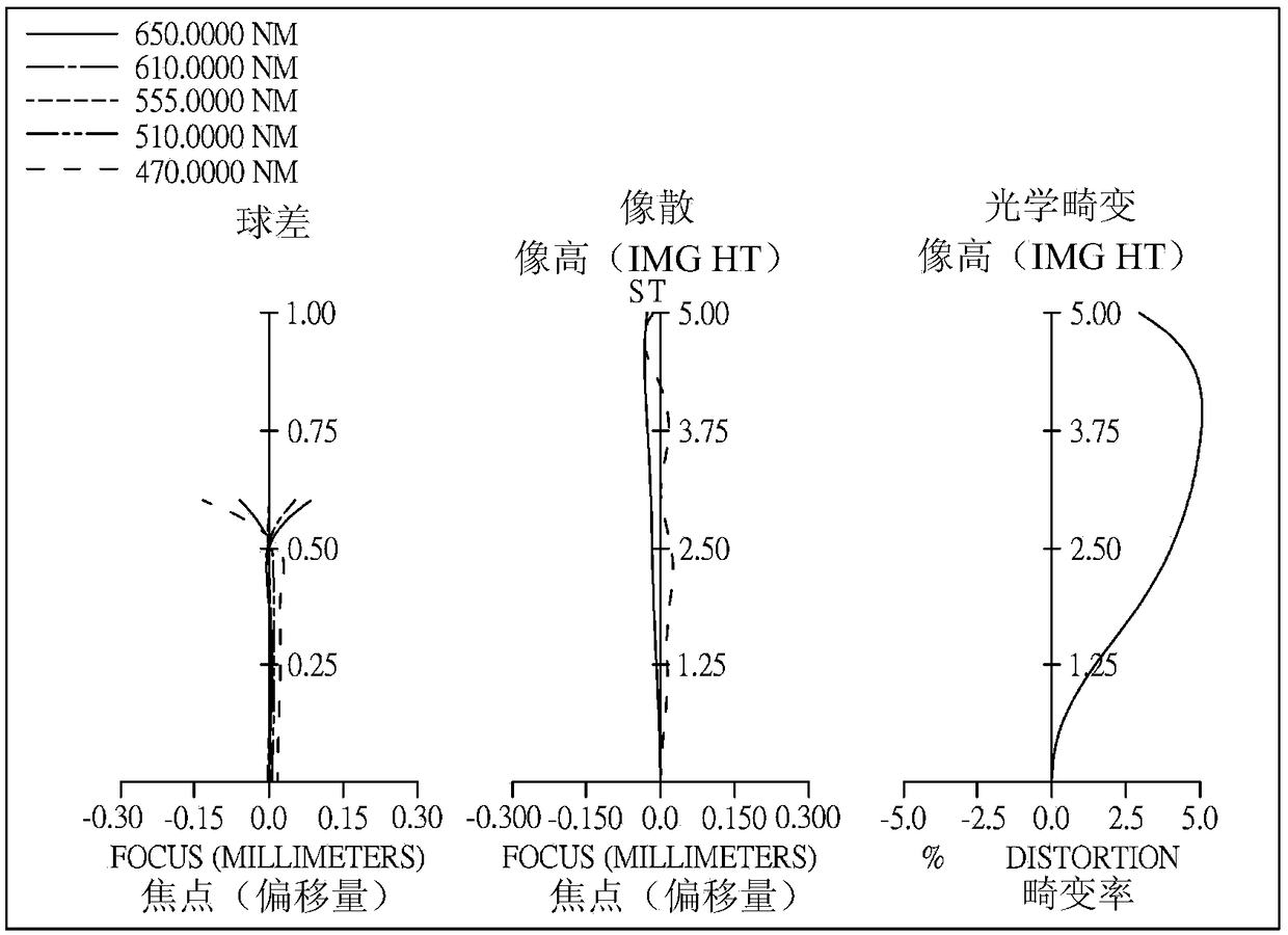
[0207] Please refer to Figure 1A and Figure 1B ,among them Figure 1A Shows a schematic diagram of an optical imaging system according to the first embodiment of the present invention, Figure 1B From left to right are the spherical aberration, astigmatism and optical distortion curves of the optical imaging system of the first embodiment. Figure 1C It is the transverse aberration diagram of the meridian surface light fan and the sagittal surface light fan of the optical imaging system of the first embodiment, the longest working wavelength and the shortest working wavelength pass through the edge of the aperture at the 0.7 field of view. by Figure 1A It can be seen that, from the object side to the image side, the optical imaging system 10 includes a first lens 110, an aperture 100, a second lens 120, a third lens 130, a fourth lens 140, a fifth lens 150, a sixth lens 160, and an infrared filter. Sheet 180, imaging surface 190, and image sensing element 192.
[0208] The first l...
no. 2 example
[0275] Please refer to Figure 2A and Figure 2B ,among them Figure 2A Shows a schematic diagram of an optical imaging system according to the second embodiment of the present invention, Figure 2B From left to right, the spherical aberration, astigmatism and optical distortion curves of the optical imaging system of the second embodiment are shown in sequence. Figure 2C This is a lateral aberration diagram of the optical imaging system of the second embodiment at a field of view of 0.7. by Figure 2A It can be seen that the optical imaging system 20 includes an aperture 200, a first lens 210, a second lens 220, a third lens 230, a fourth lens 240, a fifth lens 250, a sixth lens 260, and an infrared filter in sequence from the object side to the image side. Sheet 280, imaging surface 290, and image sensing element 292.
[0276] The first lens 210 has positive refractive power and is made of plastic material. Its object side surface 212 is convex, and its image side surface 214 i...
no. 3 example
[0300] Please refer to Figure 3A and Figure 3B ,among them Figure 3A Shows a schematic diagram of an optical imaging system according to the third embodiment of the present invention, Figure 3B From left to right are graphs of spherical aberration, astigmatism and optical distortion of the optical imaging system of the third embodiment. Figure 3C This is a lateral aberration diagram of the optical imaging system of the third embodiment at a field of view of 0.7. by Figure 3A It can be seen that the optical imaging system 30 includes an aperture 300, a first lens 310, a second lens 320, a third lens 330, a fourth lens 340, a fifth lens 350, a sixth lens 360, and an infrared filter in order from the object side to the image side. Sheet 380, imaging surface 390, and image sensing element 392.
[0301] The first lens 310 has positive refractive power and is made of plastic material. Its object side surface 312 is a convex surface, and its image side surface 314 is a convex surfa...
PUM
 Abstract
Description
Claims
Application Information
 - R&D
- Intellectual Property
- Life Sciences
- Materials
- Tech Scout
- Unparalleled Data Quality
- Higher Quality Content
- 60% Fewer Hallucinations
Browse by: Latest US Patents, China's latest patents, Technical Efficacy Thesaurus, Application Domain, Technology Topic, Popular Technical Reports.
© 2025 PatSnap. All rights reserved.Legal|Privacy policy|Modern Slavery Act Transparency Statement|Sitemap|About US| Contact US: help@patsnap.com


