
Substrate and substrate-applying welding structure and welding method

A welding method and welding structure technology, which are applied to electrical components, electric solid devices, circuits, etc., can solve the problems of short circuit and difficult to manufacture, and achieve the effects of improving production efficiency, low production cost and simple welding method.

Inactive Publication Date: 2017-01-25
INNOLIGHT TECHNOLOGY (SUZHOU) LTD
View PDF4 Cites 7 Cited by
  • Summary
  • Abstract
  • Description
  • Claims
  • Application Information

AI Technical Summary

Problems solved by technology

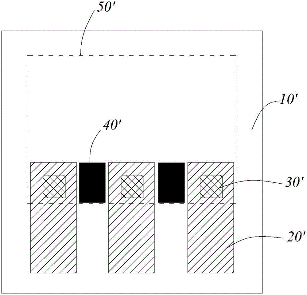
However, since metal nickel is a conductive material and polyimide is an insulating material, if the size between pads is too small, metal nickel is difficult to solve the problem of preventing tin overflow and short circuit between pads, and polyimide material is difficult to process The line spacing is less than 50μm, so it is difficult to manufacture the pad spacing below 50μm

Method used


Image

  • Substrate and substrate-applying welding structure and welding method
  • Substrate and substrate-applying welding structure and welding method
  • Substrate and substrate-applying welding structure and welding method

Examples


Embodiment Construction

[0025] The application will be described in detail below in conjunction with specific implementations shown in the accompanying drawings. However, these implementations do not limit the present application, and any structural, method, or functional changes made by those skilled in the art based on these implementations are included in the protection scope of the present application.

[0026] In each drawing of the present application, some dimensions of structures or parts are exaggerated relative to other structures or parts for the convenience of illustration, and therefore, are only used to illustrate the basic structure of the subject matter of the present application.

[0027] The terms used herein to denote relative spatial positions such as "upper", "above", "under", "under", etc. are for convenience of description to describe the relative position of one element or feature relative to another as shown in the drawings. Relationships of units or features. The terms of s...


PUM


Abstract

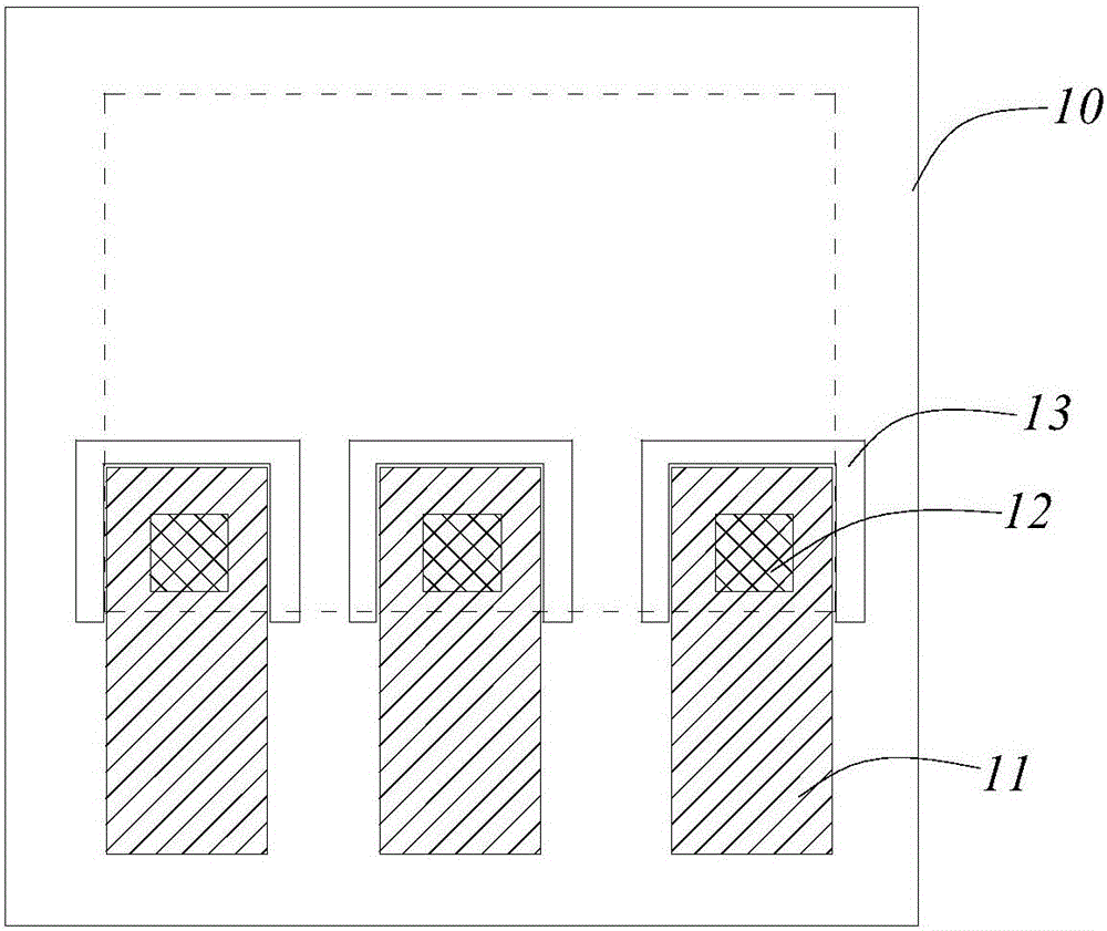
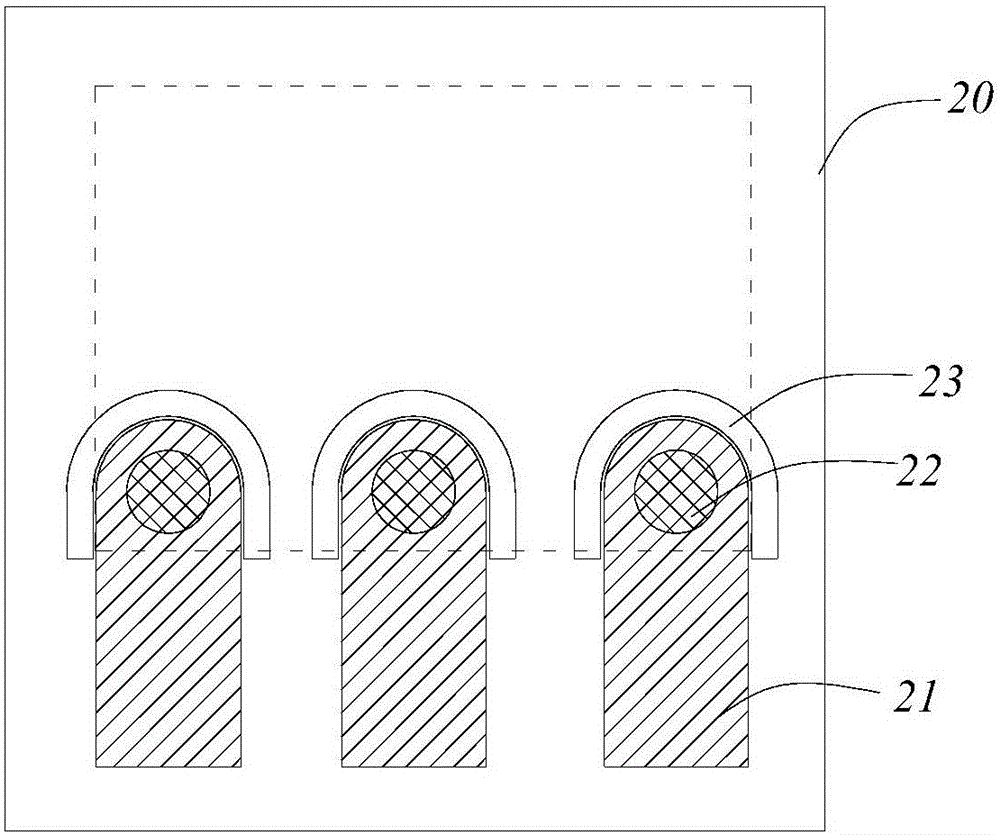
The invention discloses a substrate and a substrate-applying welding structure and a welding method. The substrate is a semiconductor substrate, wires and bonding pads are arranged on the semiconductor substrate, the wires are used for transmitting electric signals, the bonding pads are electrically connected with the wires and used for welding of external devices, and the semiconductor substrate is provided with welding-resistant grooves close to outer sides of the bonding pads. By the welding-resistant grooves in the outer sides of the bonding pads, excessive welding flux can be absorbed by the welding-resistant grooves in a welding process, so that overflowing of the welding flux is prevented. The semiconductor substrate is adopted, high-precision welding-resistant grooves can be made by means of photoetching and etching, and applicability to substrates with wire spacing being 50micron or below is realized.

Description

technical field [0001] The invention belongs to the technical field of microelectronic welding, and in particular relates to a substrate, a welding structure and a welding method using the substrate. Background technique [0002] In the prior art, the chip and the substrate (glass or ceramics) can be electrically connected by soldering processes such as gold tin. As the distance between the two pads is getting smaller and smaller, due to the heating and pressure of gold and tin during the soldering process, the molten solder tends to overflow to the surroundings, which is easy to short circuit with the surrounding pads. [0003] ginseng figure 1 As shown, the substrate 10' is provided with a wire 20', and the wire 20' is provided with a pad 30', and the chip 50' is electrically connected to the circuit layer through the pad 30'. At present, the substrate 10' is generally made of ceramics or glass, and the wires 20' and pads 30' (gold-tin) are made by photolithography and s...

Claims


Application Information

Patent Timeline
Patent Type & Authority Applications(China)
IPC IPC(8): H01L23/488H01L21/60
Inventor 汪振中孙雨舟
Owner INNOLIGHT TECHNOLOGY (SUZHOU) LTD
Learn More