Device for reducing growth of back of wafer

A backside and wafer technology, applied in gaseous chemical plating, coating, electrical components, etc., can solve problems affecting wafer leveling, affecting photoresist exposure defocus and OVL transformation, etc.

Inactive Publication Date: 2017-01-25
SHANGHAI HUALI MICROELECTRONICS CORP
View PDF3 Cites 2 Cited by
  • Summary
  • Abstract
  • Description
  • Claims
  • Application Information

AI Technical Summary

Problems solved by technology

Due to the residue of silicon nitride SIN on the back of the wafer, it affects the leveling of the wafer, which in turn affects the defocus and OVL transition of the photoresist exposure process in the subsequent process.

Method used


Image

  • Device for reducing growth of back of wafer
  • Device for reducing growth of back of wafer
  • Device for reducing growth of back of wafer

Examples


Embodiment Construction

[0021] In order to make the content of the present invention clearer and easier to understand, the content of the present invention will be described in detail below in conjunction with specific embodiments and accompanying drawings.

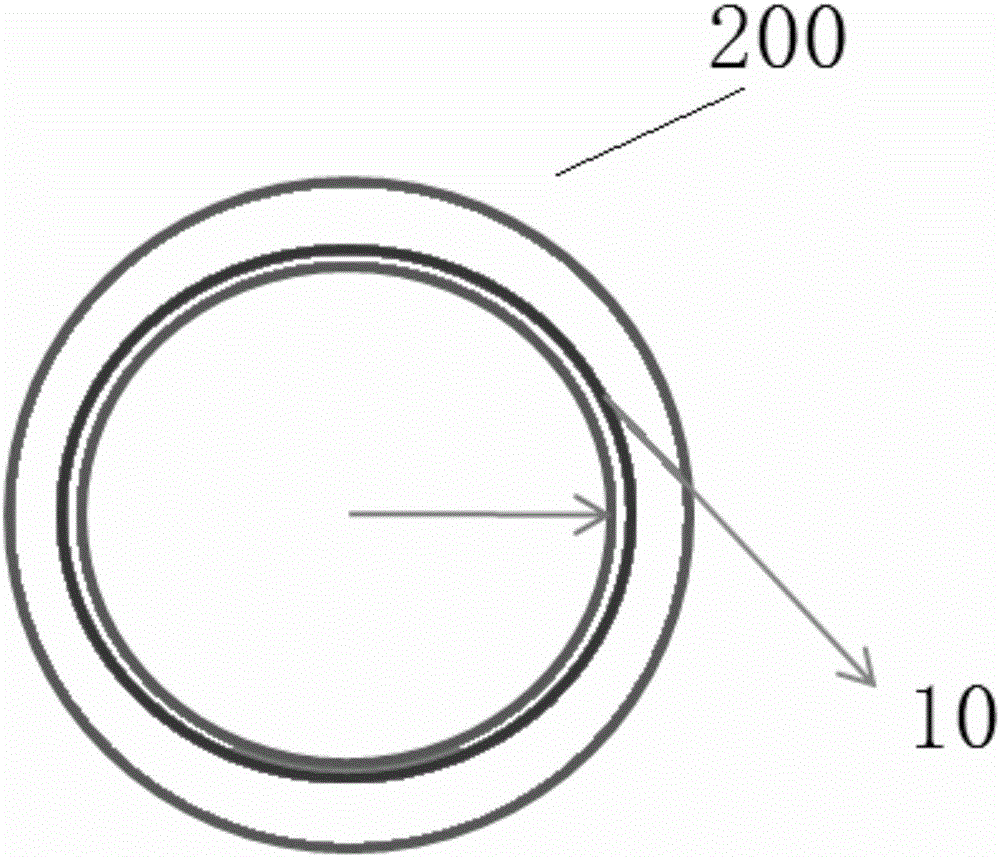
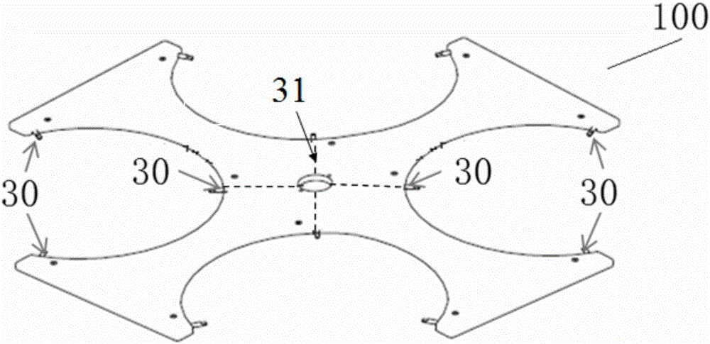
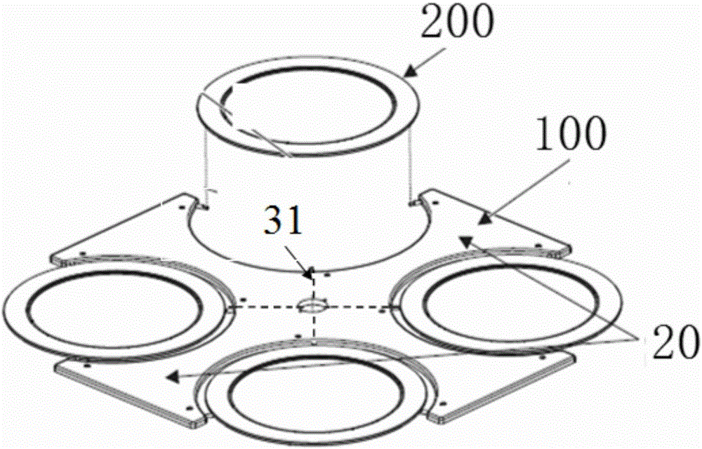
[0022] On the existing Novellus vector series machines, due to the defects in the machine design, the oxide grown by the atomic layer deposition method grows not only on the front side of the wafer, but also on the back side of the wafer. The growth of oxides brings many unnecessary problems to the follow-up. In view of this, the present invention can avoid the growth on the back side of the wafer by improving various structures. When the atomic layer precipitated oxide is grown under the device of the present invention, there will be no residue of the atomic layer precipitated oxide on the back of the wafer, so that the problems of defocus and OVL transformation in the photoresist exposure process of the subsequent process will not be affected....


PUM

PropertyMeasurementUnit
widthaaaaaaaaaa

Abstract

The invention provides a device for reducing the growth on the back of the wafer, comprising: a transfer plate, a load ring mounted on the transfer plate, and a vacuum device; wherein, a circular groove concentric with the load ring is formed on the panel of the load ring Grooves; vent holes for venting toward the load ring are arranged on each load ring mounting site on the transfer plate, wherein the vacuum device communicates with the vent holes. In the present invention, during the growth process of the oxide, the wafer is sucked on the load ring by means of a vacuum device, so that there is no gap between the wafer and the load ring, so that the reaction source cannot flow into the back of the wafer and Oxide no longer grows.

Description

technical field [0001] The invention relates to the field of semiconductor manufacturing, and more specifically, the invention relates to a device for reducing growth on the back side of a wafer. Background technique [0002] With the development of semiconductor technology, Atomic Layer Deposition (ALD) technology has been increasingly used in the industry due to its strong hole filling ability, good step coverage, low temperature, and high retention. [0003] However, for atomic layer precipitated oxides grown on Novellus vector series machines, due to the defects in the machine design, the reaction source can enter the back of the wafer, resulting in the growth of the front side of the wafer and the growth of the back side of the wafer. , Due to the problem of the reactant used, the oxide grown on the edge (edge) on the back of the wafer is thick, while the center (center) on the back of the wafer does not grow oxide because the reaction source cannot reach it. In this w...

Claims


Application Information

Patent Timeline
Patent Type & Authority Applications(China)
IPC IPC(8): H01L21/683C23C16/40C23C16/458
CPCH01L21/6838C23C16/40C23C16/458C23C16/4581
Inventor 刘春文
Owner SHANGHAI HUALI MICROELECTRONICS CORP
Why Eureka
Try Eureka