
Microscopic scanning imaging acquisition device for vertical optical element surface damage and method thereof

An optical element, scanning imaging technology, applied in measurement devices, optical testing of flaws/defects, material analysis by optical means, etc., can solve the problem that the position and attitude repeatability of optical elements are not easy to guarantee, affect the reliability of experimental data, and place components. High attitude requirements, etc., to achieve high-precision image stitching and damage detection, to achieve the effect of online rapid damage detection

Inactive Publication Date: 2017-01-18
INST OF AUTOMATION CHINESE ACAD OF SCI
View PDF5 Cites 11 Cited by
  • Summary
  • Abstract
  • Description
  • Claims
  • Application Information

AI Technical Summary

Problems solved by technology

The disadvantages of existing commercial microscopes are that they can only be used for offline detection, the detection efficiency is too low, the requirements for component placement are extremely high, the splicing accuracy is poor, and the price is expensive
In addition, frequent installation makes it difficult to ensure the repeatability of the position and attitude of optical components in the optical path, which affects the reliability of experimental data to a certain extent

Method used


Image

  • Microscopic scanning imaging acquisition device for vertical optical element surface damage and method thereof
  • Microscopic scanning imaging acquisition device for vertical optical element surface damage and method thereof

Examples


Embodiment Construction

[0021] In order to make the object, technical solution and advantages of the present invention clearer, the present invention will be described in further detail below in conjunction with specific embodiments and with reference to the accompanying drawings.

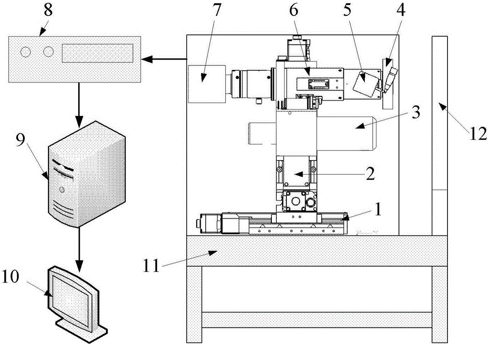
[0022] figure 1 It is a three-dimensional diagram of a microscopic scanning imaging collection device for vertical optical elements disclosed in an embodiment of the present invention, figure 2 It is a flowchart of the work of the vertical optical element microscopic scanning imaging acquisition device in an embodiment of the present invention, such as figure 1 As shown, the device of the present invention includes: a two-dimensional scanning motion platform 2, a one-dimensional focusing axis 1, an automatic zoom microscope lens 6, an area array color CCD 7, a coaxial light source 5, a ring light source 4, and a dispersion confocal displacement sensor 3 , system controller 8, industrial computer 9, shock-isolation platf...


PUM


Abstract

The invention discloses a microscopic scanning imaging acquisition device for vertical optical element surface damage and a method thereof. The device comprises a two-dimensional scanning motion platform, a one-dimensional focusing shaft, a automatic zoom microscope, a area array color CCD, a coaxial light source, a ring light source, a dispersion confocal displacement sensor, a system controller, an industrial control computer, a seismic isolation platform and a display. The device of the invention can automatically acquire and store images, can automatically complete image splicing, has image analysis capability, and can count quantity and dimension of damage spots in an image. According to the invention, online rapid high-precision microscopic scanning imaging acquisition and damage detection of vertical optical element surface in an optical path can be realized. The device of the invention has a wide application prospect and considerable social and economic benefits.

Description

technical field [0001] The invention relates to the field of surface damage detection of optical components, in particular to a microscopic scanning imaging acquisition device and method for surface damage of vertical optical components. Background technique [0002] In the optical experiment, there is a kind of damage test experiment, which needs to test the damage degree of the laser intensity to the optical element. Because the detection accuracy of the damage size is relatively strict, it must be realized with the help of a high-magnification microscope for magnified imaging and splicing. The disadvantages of existing commercial microscopes are that they can only be used for offline detection, the detection efficiency is too low, the requirements for component placement are extremely high, the splicing accuracy is poor, and the price is expensive. In addition, frequent installation makes it difficult to ensure the repeatability of the position and attitude of optical com...

Claims


Application Information

Patent Timeline
Patent Type & Authority Applications(China)
IPC IPC(8): G01N21/95G01N21/958
CPCG01N21/95G01N21/958G01N2021/9511G01N2201/103G01N2201/108
Inventor 史亚莉张正涛陶显徐德
Owner INST OF AUTOMATION CHINESE ACAD OF SCI
Learn More