A kind of oled display panel and its preparation method, testing method

A technology for display panels and display areas, applied in static indicators, semiconductor/solid-state device manufacturing, instruments, etc., can solve the problems of easy scratches on the edges of metal films, poor dark lines, and circuit scratches

Active Publication Date: 2018-01-12
BOE TECH GRP CO LTD
View PDF3 Cites 0 Cited by
  • Summary
  • Abstract
  • Description
  • Claims
  • Application Information

AI Technical Summary

Problems solved by technology

[0004] In the evaporation process, a mask plate is needed, and the mask plate is easy to scratch the circuit on the array substrate located in the peripheral wiring area and close to the edge of the array substrate during the alignment process, resulting in When the panel is performing a lighting test, there is a dark line defect
In addition, when packaging, if metal packaging is used, the edge of the metal film will easily scratch the circuit on the array substrate located in the peripheral wiring area and close to the edge of the array substrate during the alignment process.

Method used


Image

  • A kind of oled display panel and its preparation method, testing method
  • A kind of oled display panel and its preparation method, testing method
  • A kind of oled display panel and its preparation method, testing method

Examples


Embodiment Construction

[0026] The following will clearly and completely describe the technical solutions in the embodiments of the present invention with reference to the accompanying drawings in the embodiments of the present invention. Obviously, the described embodiments are only some, not all, embodiments of the present invention. Based on the embodiments of the present invention, all other embodiments obtained by persons of ordinary skill in the art without making creative efforts belong to the protection scope of the present invention.

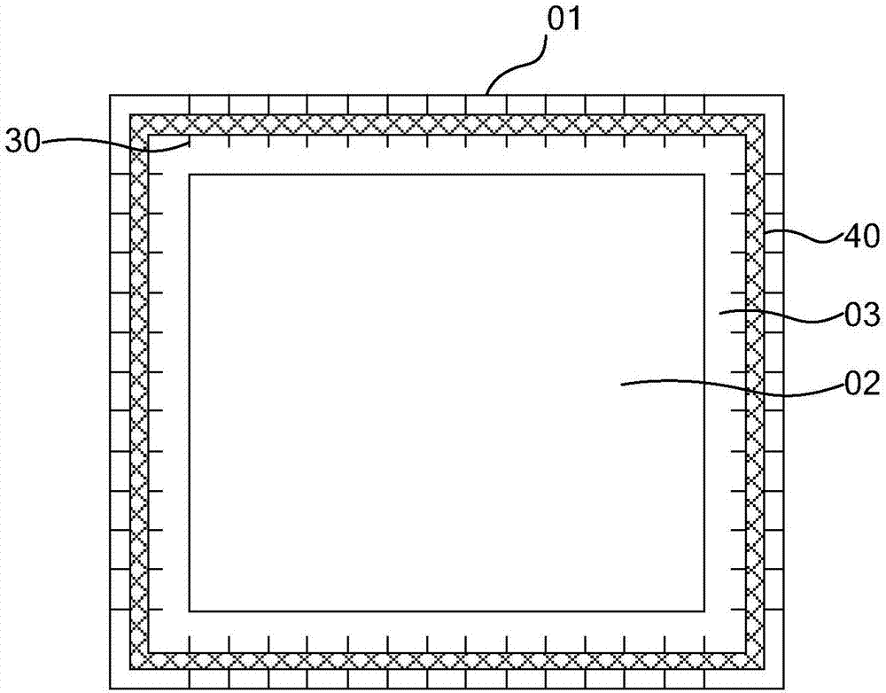
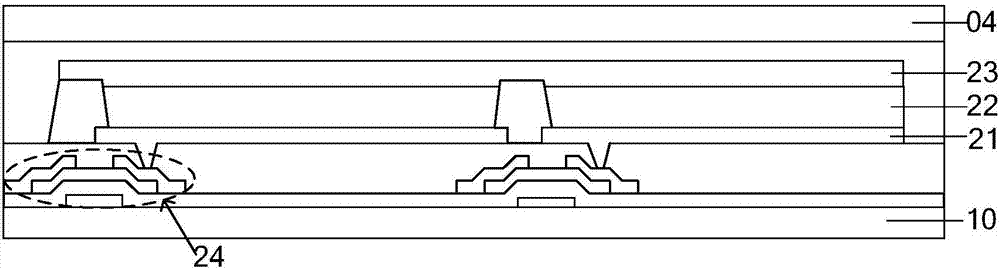
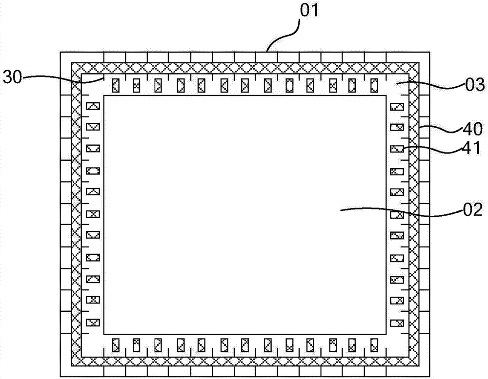
[0027] An embodiment of the present invention provides an OLED display panel, such as figure 1 and figure 2 As shown, it includes an array substrate 01 and a packaging cover plate 04. The array substrate 01 includes a display area 02 and a peripheral wiring area 03; the peripheral wiring area 03 includes a circuit 30 arranged on the edge of the array substrate 01, and an Conductive rubber strip 40; the conductive rubber strip 40 extends along the direction o...


PUM


Abstract

Embodiments of the present invention provide an OLED display panel and its preparation method and testing method, which relate to the field of display technology and can avoid scratches on circuits during the process of manufacturing the OLED display panel. The OLED display panel includes an array substrate and an encapsulation cover plate, the array substrate includes a display area and a peripheral wiring area; the peripheral wiring area includes a circuit arranged on the edge of the array substrate, and a conductive glue arranged above the circuit strip; the conductive glue extends along the direction of the edge of the adjacent display area; wherein, the conductive glue strip is conductive in the Z direction and non-conductive in the X and Y planes; the Z direction is perpendicular to the array substrate the substrate. For OLED display devices.

Description

technical field [0001] The invention relates to the field of display technology, in particular to an OLED display panel, a preparation method and a testing method thereof. Background technique [0002] Organic Light Emitting Diode (OLED) display is an organic thin film electroluminescent device, which has the advantages of simple preparation process, low cost, easy formation of flexible structure, and wide viewing angle. Therefore, the display technology of OLEDs has become an important display technology. [0003] The OLED display includes an array substrate and a package substrate, and the array substrate includes a thin film transistor (Thin Film Transistor, TFT for short) and an OLED light-emitting device composed of an anode, an organic material functional layer and a cathode. The organic material functional layer needs to be formed by evaporation process. [0004] In the evaporation process, a mask plate is needed, and the mask plate is easy to scratch the circuit on...

Claims


Application Information

Patent Timeline
Patent Type & Authority Patents(China)
IPC IPC(8): H01L27/32H01L51/52G09G3/00
CPCG09G3/006H10K59/131H10K50/841
Inventor 王琳琳王辉锋徐攀
Owner BOE TECH GRP CO LTD
Why Eureka
Try Eureka