Semiconductor element manufacturing method

A component manufacturing and semiconductor technology, applied in the field of semiconductor component manufacturing, can solve problems such as complex steps, defects, and impact on component performance.

Inactive Publication Date: 2017-01-04
UNITED MICROELECTRONICS CORP
View PDF9 Cites 3 Cited by
  • Summary
  • Abstract
  • Description
  • Claims
  • Application Information

AI Technical Summary

Problems solved by technology

However, the steps to replace the gate manufacturing process are quite complicated, and the device is pr

Method used


Image

  • Semiconductor element manufacturing method
  • Semiconductor element manufacturing method
  • Semiconductor element manufacturing method

Examples


Embodiment Construction

[0043] The foregoing and other technical contents, features and effects of the present invention will be clearly presented in the following detailed description of a preferred embodiment with reference to the accompanying drawings. The directional terms mentioned in the following embodiments, such as: up, down, left, right, front or back, etc., are only directions referring to the attached drawings. Accordingly, the directional terms are used to illustrate and not to limit the invention.

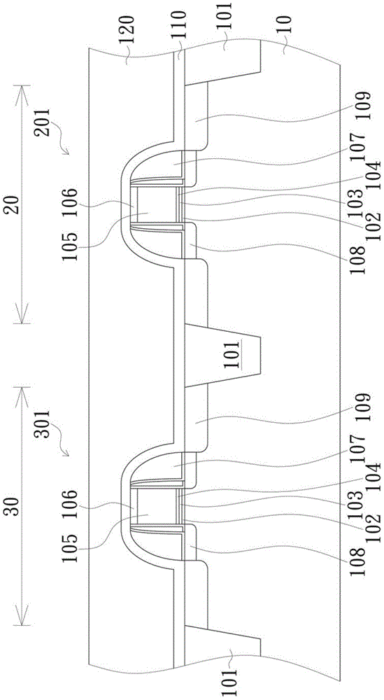
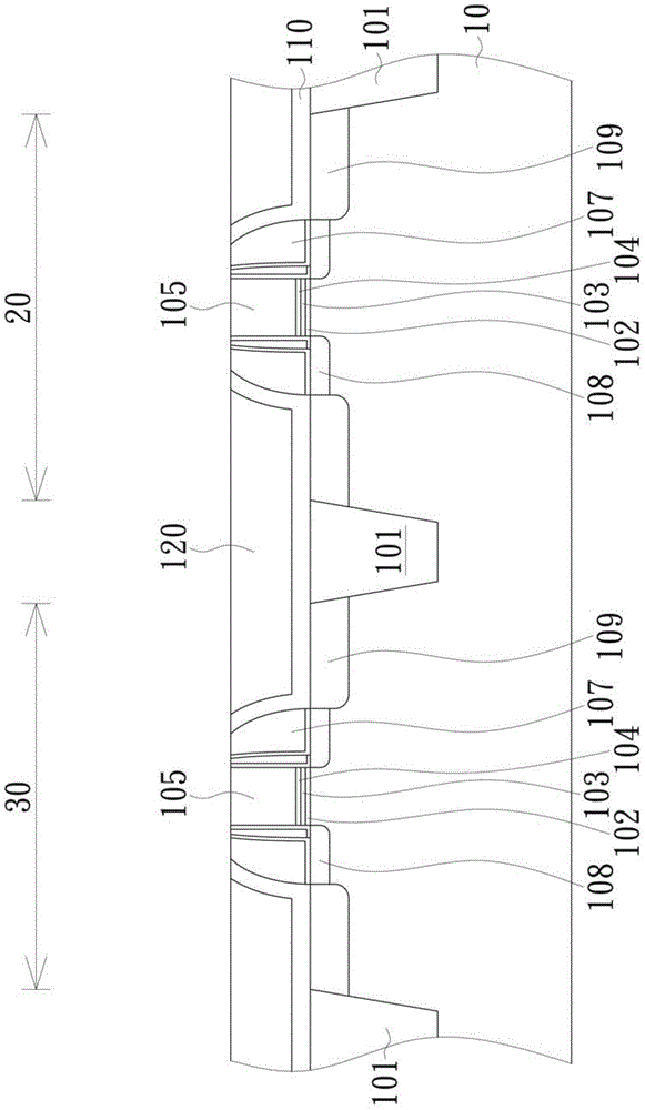
[0044] Figure 1 to Figure 8 is a schematic cross-sectional view of the manufacturing method of the semiconductor device according to the first embodiment of the present invention. First, a substrate 10 is provided, such as a silicon substrate, a silicon-containing substrate, or a silicon-on-insulator (SOI) substrate. There are a plurality of shallow trench isolations (shallow trench isolation, STI) 101 on the substrate 10, and the shallow trench isolations 101 can have proper stress. The...


PUM


Abstract

The present invention discloses a semiconductor element manufacturing method. First, a substrate with a first transistor structure and a second transistor structure is provided, wherein the first transistor structure is provided with a first gate trench, and the second transistor structure is provided with a second gate trench. Then, a first work function metal layer is formed in the first gate trench and the second gate trench, and a flat layer is formed on the first work function metal layer. Then, a patterned photoresist layer is formed on the flat layer, and a part of the flat layer on the second transistor structure is etched. Then, after the patterned photoresist layer is removed, the flat layer is fully etched until the flat layer on the second transistor structure is completely removed, and a patterned flat layer is kept to cover the first transistor structure. Finally, the first work function metal layer in the second gate trench is removed.

Description

technical field [0001] The invention relates to a method for manufacturing a semiconductor element, in particular to a method for manufacturing a semiconductor element with a metal gate. Background technique [0002] As the size of semiconductor devices shrinks day by day, the size of the gate structure also shrinks accordingly. Therefore, the thickness of the gate dielectric layer must also be reduced to avoid affecting device performance. Generally speaking, the material of the gate dielectric layer is usually silicon oxide. The gate dielectric layer made of silicon oxide tends to have a leakage current when its thickness is reduced. In order to reduce the occurrence of leakage current, the current practice is to replace silicon oxide with a high dielectric constant (high dielectric constant; high-k) material as the gate dielectric layer. In the case of using a high dielectric constant material as the gate dielectric layer, the gate made of polysilicon will react with t...

Claims


Application Information

Patent Timeline
IPC IPC(8): H01L21/8234H01L21/28
CPCH01L21/8234H01L21/823431H01L21/82345H01L29/401
Inventor 杨宗杰
Owner UNITED MICROELECTRONICS CORP
Why Eureka
Try Eureka