
Organic light-emitting display panel and organic light-emitting display device

A light-emitting display and organic technology, applied in instruments, semiconductor devices, computing, etc., can solve the problems of increasing production costs, increasing the thickness of display devices, and increasing the process steps of piezo-sensitive capacitor film layers, so as to reduce production costs and process difficulty , the effect of reducing the thickness

Active Publication Date: 2016-12-07
SHANGHAI TIANMA MICRO ELECTRONICS CO LTD +1
View PDF7 Cites 13 Cited by
  • Summary
  • Abstract
  • Description
  • Claims
  • Application Information

AI Technical Summary

Problems solved by technology

[0003] In the process of making the above-mentioned pressure-sensitive display device, it is necessary to increase the process steps of making the pressure-sensitive capacitance film layer, thereby increasing the production cost; and, due to the increase of the film layer structure, the thickness of the display device may be increased, which is not conducive to flexible display. Thinning and Lightening of Devices
In addition, the existing pressure-sensitive display devices are designed for rigid display panels and cannot be applied to flexible display devices.

Method used


Image

  • Organic light-emitting display panel and organic light-emitting display device
  • Organic light-emitting display panel and organic light-emitting display device
  • Organic light-emitting display panel and organic light-emitting display device

Examples


Embodiment Construction

[0018] The application will be further described in detail below in conjunction with the accompanying drawings and embodiments. It should be understood that the specific embodiments described here are only used to explain related inventions, rather than to limit the invention. It should also be noted that, for the convenience of description, only the parts related to the related invention are shown in the drawings.

[0019] It should be noted that, in the case of no conflict, the embodiments in the present application and the features in the embodiments can be combined with each other. The present application will be described in detail below with reference to the accompanying drawings and embodiments.

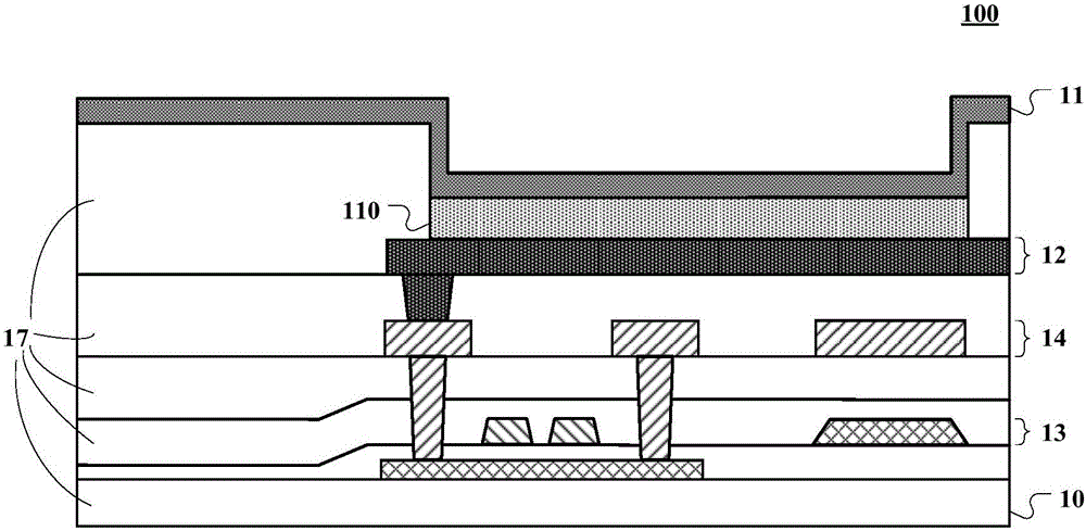
[0020] The realization of the pressure-sensitive function of the organic light-emitting display panel provided by each embodiment of the present application is designed based on the structure of the existing organic light-emitting display panel. The following first refers to ...


PUM

PropertyMeasurementUnit
Elastic modulusaaaaaaaaaa
Thicknessaaaaaaaaaa

Abstract

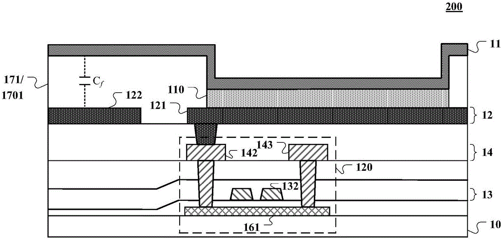
The invention discloses an organic light-emitting display panel and an organic light-emitting display device. The organic light-emitting display panel comprises a substrate, a cathode layer, an anode layer, a plurality of metal layers and an insulating medium, wherein the anode layer is located between the substrate and the cathode layer; the plurality of metal layers are located between the substrate and the anode layer; the insulating medium is located between the metal layers and the cathode layer; the anode layer comprises an anode region; the cathode layer is multiplexed as a first pressure-sensitive electrode; a second pressure-sensitive electrode is arranged on the metal layer or in a region not overlapping with the anode region of the anode layer; and the first pressure-sensitive electrode, the second pressure-sensitive electrode and the insulating medium located between the first pressure-sensitive electrode and the second pressure-sensitive electrode are used for sensing pressure. The organic light-emitting display panel and the organic light-emitting display device can achieve pressure sensing on the basis of an existing organic light-emitting display panel; the manufacturing cost is reduced; and the thickness of a pressure-sensitive display device is reduced.

Description

technical field [0001] The present application relates to the field of display technology, specifically to the field of organic light-emitting display technology, and in particular to an organic light-emitting display panel and an organic light-emitting display device. Background technique [0002] With the development of display technology, display devices with pressure-sensitive functions are more and more widely used. In existing pressure-sensitive display devices, the realization of the pressure-sensitive function usually requires adding a film structure between the backlight unit of the liquid crystal display and the array substrate, or adding a film structure around the organic light-emitting display to form a pressure-sensitive Capacitance, which converts pressure into changes in piezo-capacitance, so as to detect pressure by sensing the change in piezo-capacitance. [0003] In the process of making the above-mentioned pressure-sensitive display device, it is necessa...

Claims


Application Information

Patent Timeline
IPC IPC(8): H01L27/32G06F3/041G06F3/044
CPCG06F3/0414G06F3/044G06F2203/04102H10K59/40H10K59/12H10K59/131H10K77/111
Inventor 冷传利霍思涛
Owner SHANGHAI TIANMA MICRO ELECTRONICS CO LTD
Learn More