Method for forming fin field effect transistor

A fin field effect and transistor technology, which is applied in semiconductor/solid-state device manufacturing, electrical components, circuits, etc., can solve the problems that the performance of fin field effect transistors needs to be improved

Active Publication Date: 2019-09-27
SEMICON MFG INT (SHANGHAI) CORP
View PDF4 Cites 0 Cited by
  • Summary
  • Abstract
  • Description
  • Claims
  • Application Information

AI Technical Summary

Problems solved by technology

[0005] However, the performance of fin field effect transistors formed by existing technologies still needs to be improved.

Method used


Image

  • Method for forming fin field effect transistor
  • Method for forming fin field effect transistor
  • Method for forming fin field effect transistor

Examples


Embodiment Construction

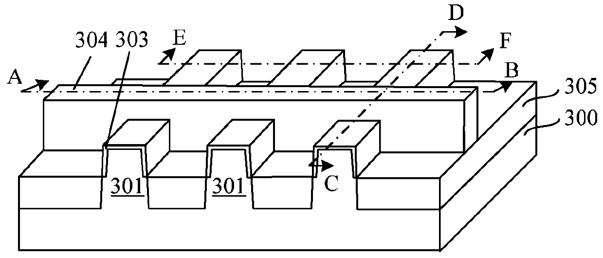
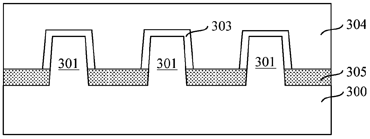
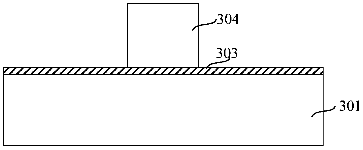
[0035] As mentioned in the background technology, the performance of the fin field effect transistor formed by the prior art still needs to be improved, for example, the stress exerted by the stress source region and the drain region on the channel region of the fin field effect transistor formed by the prior art is still relatively limited .

[0036] The formation process of the prior art fin field effect transistor is studied, including: providing a semiconductor substrate on which a raised fin is formed; forming a sidewall and a top surface across a portion of the fin The gate structure includes a gate dielectric layer located on the sidewall and top surface of the fin and a gate electrode located on the gate dielectric layer, the material of the gate dielectric layer is silicon oxide, and the formation process is thermal Oxidation, the material of the gate electrode is polysilicon; Re-oxidize the sidewall of the gate electrode to repair the etching damage; Form an offset s...


PUM


Abstract

A fin type field effect transistor forming method is disclosed and comprises the following steps: a semiconductor substrate is provided, fin parts are formed on the semiconductor substrate, first silicon oxide layers are formed on surfaces of side walls and top parts of the fin parts, and a polysilicon grid electrode is formed on parts of surfaces of the first silicon oxide layers; parts, positioned at two sides of the polysilicon grid electrode, of the first silicon oxide layers arranged on surfaces of the fin parts are removed; side walls of the polysilicon grid electrode is cleaned via an ozone-containing solution, a second silicon oxide layer is formed on surfaces of the side walls of the polysilicon grid electrode, offset side walls are formed on surfaces of side walls of the second silicon oxide layer, and the polysilicon grid electrode and the offset side walls are mask layers; parts, positioned on two sides of the polysilicon grid electrode and the offset side walls, of the fin parts are etched; grooves are formed, and stress source / drain regions are formed in the grooves. Via the fn type field effect transistor forming method, performance of the formed source / drain regions can be improved.

Description

technical field [0001] The invention relates to the field of semiconductor manufacturing, in particular to a method for forming a fin field effect transistor. Background technique [0002] With the continuous development of semiconductor process technology, process nodes are gradually reduced, and gate-last (gate-last) process has been widely used to obtain an ideal threshold voltage and improve device performance. However, when the feature size (CD, Critical Dimension) of the device is further reduced, even if the gate-last process is adopted, the structure of the conventional MOS field effect transistor can no longer meet the requirements for device performance, and the fin field effect transistor (Fin FET) as a conventional Device substitution has received extensive attention. [0003] A fin field effect transistor in the prior art includes: a semiconductor substrate on which protruding fins are formed, and the fins are generally obtained by etching the semiconductor sub...

Claims


Application Information

Patent Timeline
Patent Type & Authority Patents(China)
IPC IPC(8): H01L21/336
Inventor 丁士成
Owner SEMICON MFG INT (SHANGHAI) CORP
Why Eureka
Try Eureka