
Hexagonal phase epitaxial cadmium sulfide on copper indium gallium selenide for a photovoltaic junction

一种硒化铜铟镓、硫化镉的技术,应用在光伏发电、电气元件、气候可持续性等方向,能够解决化学浴沉积方法整合、不是可行等问题

Active Publication Date: 2016-11-23
BEIJING APOLLO DING RONG SOLAR TECH +4
View PDF8 Cites 4 Cited by
  • Summary
  • Abstract
  • Description
  • Claims
  • Application Information

AI Technical Summary

Problems solved by technology

However, for vacuum-deposited CIGS films, the chemical bath deposition method may not be a feasible solution
It is practically impossible to integrate chemical bath deposition methods into roll-to-roll or continuous deposition methods for depositing thin-film solar cell materials

Method used


Image

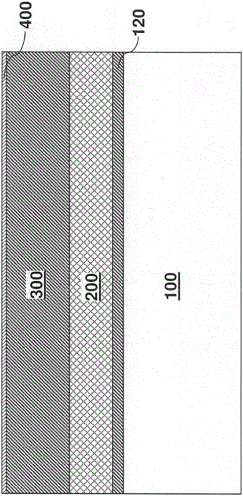
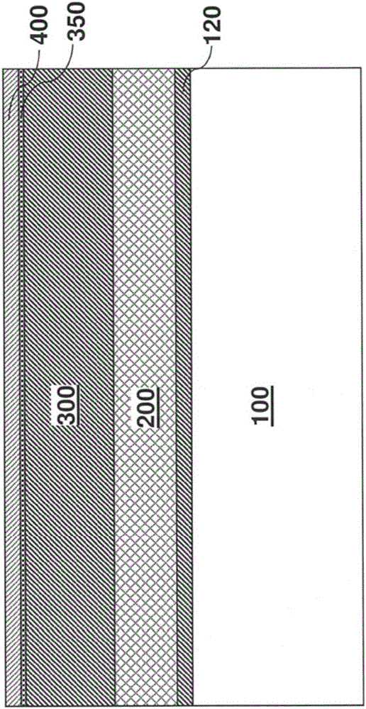
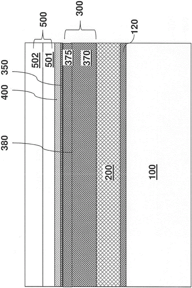
  • Hexagonal phase epitaxial cadmium sulfide on copper indium gallium selenide for a photovoltaic junction
  • Hexagonal phase epitaxial cadmium sulfide on copper indium gallium selenide for a photovoltaic junction
  • Hexagonal phase epitaxial cadmium sulfide on copper indium gallium selenide for a photovoltaic junction

Examples


example

[0115] By using advanced scanning transmission electron microscopy (STEM) combined with energy dispersive X-ray spectroscopy (EDS), the present inventors systematically investigated the simultaneous transfer of hydrogen and oxygen by magnetron sputtering on moving substrates as described above. Both were introduced into several different PVD-CdS / CIGS heterojunctions fabricated in the processing chamber. The main difference in heterojunctions is the different oxygen content used in the sputtering gas during the PVD cadmium sulfide deposition process.

[0116] Table I shows that in CdS process with different O 2 Performance of measurements of four different CdS / CIGS devices in concentrations. G19 (with highest O 2 ) delivered the lowest efficiency, while G21 (without O 2 ) show better performance. O in CdS 2 With an increase, device performance gradually improved as seen in the G20 and G25 devices before decreasing at the highest level. This suggests that the moderate inco...


PUM

PropertyMeasurementUnit
particle diameteraaaaaaaaaa

Abstract

A method of manufacturing a photovoltaic structure includes forming a p-type semiconductor absorber layer containing a copper indium gallium selenide based material over a first electrode, forming a n-type cadmium sulfide layer over the p-type semiconductor absorber layer by sputtering in an ambient including hydrogen gas and oxygen gas, and forming a second electrode over the cadmium sulfide layer.

Description

[0001] Statement Regarding Federally Sponsored Research or Development [0002] This invention was made with Government support under Grant No. CPS25853 awarded by the Department of Energy through the DOE / EERE SunShot BRIDGE program. The government has certain rights in this invention. technical field [0003] The present invention relates generally to the field of photovoltaic devices, and more particularly to thin film solar cells comprising photovoltaic heterojunctions between cadmium sulfide and copper indium gallium selenide. Background technique [0004] Based on CuIn 1-x Ga x Se 2 (CIGS) thin-film solar cells continue to show promise in the renewable energy market due to the steady increase in their solar conversion efficiencies in commercial-scale installations. Cadmium sulfide is a thin-film material used in conjunction with CIGS-based thin-film solar cells. An n-type cadmium sulfide layer is provided between the p-type absorber layer (eg implemented as a CIGS...

Claims


Application Information

Patent Timeline
Patent Type & Authority Applications(China)
IPC IPC(8): H01L31/18H01L31/032
CPCH01L31/0324H01L21/02557H01L31/0296H01L31/036H01L31/1828H01L21/02485H01L21/02631Y02E10/541Y02E10/543H01L31/0749H01L31/18Y02E10/547Y02P70/50
Inventor 贺小庆安格斯·罗基特乔尔·瓦利文森索·洛尔迪尼尔·麦凯乔迪·扎帕拉克张伟杰约翰·科森
Owner BEIJING APOLLO DING RONG SOLAR TECH
Learn More