Batch ball planting method for chip rework

A chip and batch technology, applied in the direction of semiconductor devices, electrical components, circuits, etc., can solve problems such as low success rate, damage to solder ball pads, and ball planting failure, so as to improve success rate and efficiency, improve work efficiency, and avoid The effect of uncertainty

Active Publication Date: 2018-11-09
MOBIWIRE MOBILES NINGBO
View PDF3 Cites 0 Cited by
  • Summary
  • Abstract
  • Description
  • Claims
  • Application Information

AI Technical Summary

Problems solved by technology

[0005] At present, BGA chips are becoming more and more miniaturized and dense, and the number of solder balls is increasing. The manual ball planting method adopted by the current general technology makes it more and more difficult to rework and plant balls, and there are still the following shortcomings: 1. Low efficiency : Only one BGA chip can be planted at a time. Before the ball planting process is solidified, it is necessary to visually check whether all the ball points are covered in place at any time. Otherwise, it is necessary to re-clean, position, brush tin beads or solder paste, and also need to visually confirm the effect after curing. ;2. Low success rate: The whole process is manual operation. After the chip is miniaturized and compacted, it is difficult to locate. At the same time, it is easy to shift during the process of brushing tin or solder paste, resulting in ball planting failure; 3. The chip is easily damaged : During the process of manual ball planting, repeated touching of the chip may easily cause electrostatic breakdown damage; unsuccessful ball planting, repeated tin removal will cause damage to the solder ball plate; during the use of the heat gun, due to excessive temperature or too close Cause high temperature damage; 4. The risk cost of re-use increases: if the ball is improperly planted, the damaged chip is used on the product, resulting in secondary maintenance of the product; although the ball planting is qualified, it has caused the life of the chip to be reduced due to high temperature fatigue and other factors , thereby affecting product quality and increasing risk costs

Method used


Image

  • Batch ball planting method for chip rework
  • Batch ball planting method for chip rework

Examples


Embodiment Construction

[0034] The technical solutions of the present invention will be described below in conjunction with the accompanying drawings and embodiments.

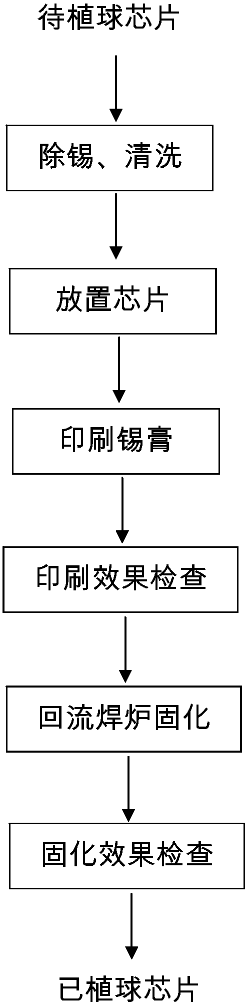
[0035] like Figure 1 to Figure 2 As shown, the present invention provides a batch ball planting method for chip rework, comprising the following steps:

[0036] 1) Desoldering and cleaning: Brush a layer of solder paste on the chip to be balled, scrape off the residual solder on the pad with a soldering iron, and clean the pad with board washing water;

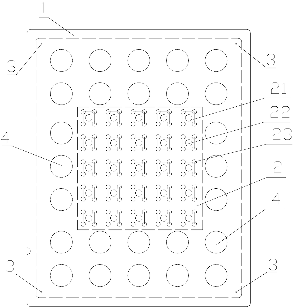
[0037] 2) Place chip: place the cleaned chip to be ball-planted in the chip placement area 2 of the batch ball-planting fixture, and then place the batch-planting ball fixture with chips on the conveyor belt of the solder paste printing machine;

[0038] 3) Printing solder paste: place the stencil corresponding to the chip to be balled on the printing machine, add solder paste, compile or call the printing machine program, turn on the printing machine, automatically load the batch b...


PUM


Abstract

The invention provides a batch ball planting method for chip rework, comprising the following steps: removing tin, cleaning, placing chips, printing solder paste, checking the printing effect, curing in a reflow oven, and checking the curing effect; Fixtures are used to realize batch ball planting of chips. The present invention designs a batch planting jig and utilizes existing solder paste printing machines, solder paste inspectors, reflow ovens and other equipment to realize batch planting of solder ball array packaging (BGA) chips, while reducing manual operations. The ball planting process is automated, and the ball planting quality is judged as equipment, thereby improving the efficiency and success rate of BGA chip ball planting. It has the advantages of batching, automation, high efficiency, high success rate, and low operating cost.

Description

technical field [0001] The invention relates to the technical field of electronic product maintenance, in particular to a batch ball planting method for chip rework. Background technique [0002] In the process of surface mount technology (SMT) production and processing, due to factors such as poor printing and patch placement, chip welding defects appear, and this phenomenon is common in various factories. Ball array package (BGA) chips are basically expensive chips such as central processing unit (CPU), flash memory (FLASH), power management, etc., and the price is tens, hundreds to thousands, and is indispensable on the circuit board of electronic products. . Due to the high price, defective chips caused by welding must be repaired and reused. At present, the ball planting rework of BGA chips basically adopts manual single ball planting, using tin beads or solder paste, and the operation methods are basically the same. [0003] Ball planting with tin beads: 1. Remove t...

Claims


Application Information

Patent Timeline
Patent Type & Authority Patents(China)
IPC IPC(8): H01L21/60
CPCH01L24/81H01L2224/81
Inventor 戴建权苏红王海东张先年
Owner MOBIWIRE MOBILES NINGBO
Why Eureka
Try Eureka