
Array substrate, display panel comprising array substrate and display device

An array substrate and display area technology, applied in the input/output process of data processing, optics, instruments, etc., can solve the problems of display panel narrow frame limitation, touch sensitivity drop, consumption of touch induced charge, etc., to achieve effective Conducive to narrow borders and reduce the effect of coupling capacitance

Active Publication Date: 2016-11-02
XIAMEN TIANMA MICRO ELECTRONICS +1
View PDF5 Cites 8 Cited by
  • Summary
  • Abstract
  • Description
  • Claims
  • Application Information

AI Technical Summary

Problems solved by technology

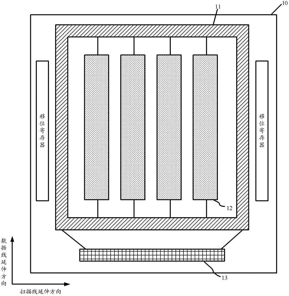
The part of the common voltage signal line 11 parallel to the shift register will form a coupling capacitor with the shift register, and the coupling capacitor will consume the touch-induced charge and reduce the touch sensitivity.
In addition, the part of the common voltage signal line parallel to the shift register will also limit the narrow border of the display panel

Method used


Image

  • Array substrate, display panel comprising array substrate and display device
  • Array substrate, display panel comprising array substrate and display device
  • Array substrate, display panel comprising array substrate and display device

Examples


Embodiment Construction

[0018] The application will be further described in detail below in conjunction with the accompanying drawings and embodiments. It should be understood that the specific embodiments described here are only used to explain related inventions, rather than to limit the invention. It should also be noted that, for ease of description, only parts related to the invention are shown in the drawings.

[0019] It should be noted that, in the case of no conflict, the embodiments in the present application and the features in the embodiments can be combined with each other. The present application will be described in detail below with reference to the accompanying drawings and embodiments.

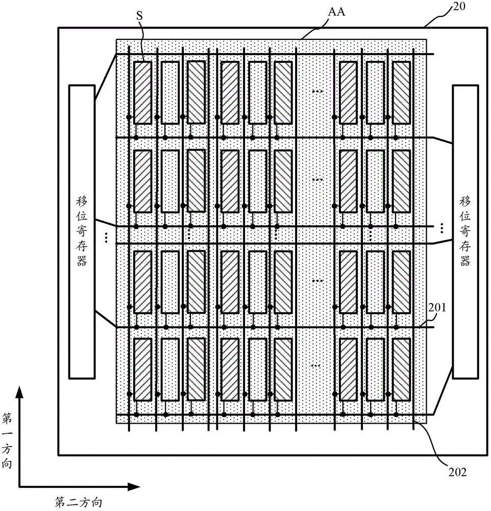
[0020] Please refer to figure 2 and image 3 , figure 2 A schematic diagram showing the relative positional relationship of the first metal electrode, the first electrode, the integrated circuit, and the shift register in an embodiment of the array substrate of the present application. image...


PUM


Abstract

The invention discloses an array substrate, a display panel comprising the array substrate and a display device, wherein the array substrate comprises a display area; the display area comprises a plurality of strip-shaped first electrodes; the first electrodes extend in the first direction and are arranged in the second direction; the array substrate is further provided with an integrated circuit; the integrated circuit is parallel with the second direction; a first metal electrode is further formed on the array substrate and is parallel with the second direction; the first metal electrode and the integrated circuit are arranged on two opposite sides of the display area; the first metal electrode is electrically connected with the integrated circuit through at least one first signal line; the first metal electrode is electrically connected with a first end to provide a public voltage signal for the first electrode during display. The first electrode originally arranged between a shifting register and the display area is eliminated, so that coupling capacitance between the first metal electrode and the shifting register is reduced, and narrow frame formation of the display panel is facilitated.

Description

technical field [0001] The present disclosure generally relates to display technology, specifically to touch display technology, and in particular to an array substrate, a display panel including the same, and a display device. Background technique [0002] In the existing mutual capacitive touch liquid crystal display panel, the common electrode is usually divided into a plurality of strip-shaped sub-common electrodes insulated from each other. In a time-division multiplexing manner, during the display period, the sub-common electrodes are common electrodes, and during the touch control period, the sub-common electrodes are multiplexed as touch electrodes. figure 1 A schematic top view of an array substrate in an existing touch display panel is shown, as shown in figure 1 As shown, the array substrate 10 includes a plurality of strip-shaped sub-common electrodes 12 . The extension direction of the sub-common electrodes 12 is often parallel to the extension direction of th...

Claims


Application Information

Patent Timeline
Patent Type & Authority Applications(China)
IPC IPC(8): G06F3/041G06F3/044G02F1/1333G02F1/1343
CPCG02F1/13338G02F1/134309G06F3/0412G06F3/0416G06F3/044G06F3/0446G06F3/0445G06F3/04184G02F1/134318G02F1/136286G02F1/133514G02F1/13454
Inventor 邹龙生潘朝煌王志杰吴树茂
Owner XIAMEN TIANMA MICRO ELECTRONICS
Learn More