A voltage-programmable amoled pixel circuit and its driving method
A technology of a pixel circuit and a driving method, applied in the field of flat display, can solve the problems of accelerating the threshold voltage and mobility of TFTs, reducing the compensation effect, process deviation, etc., and achieving the threshold voltage degradation phenomenon is slowed down, and the degradation of mobility is alleviated and reduced. effect of influence
- Summary
- Abstract
- Description
- Claims
- Application Information
AI Technical Summary
Problems solved by technology
Method used
Image
Examples
Embodiment 1
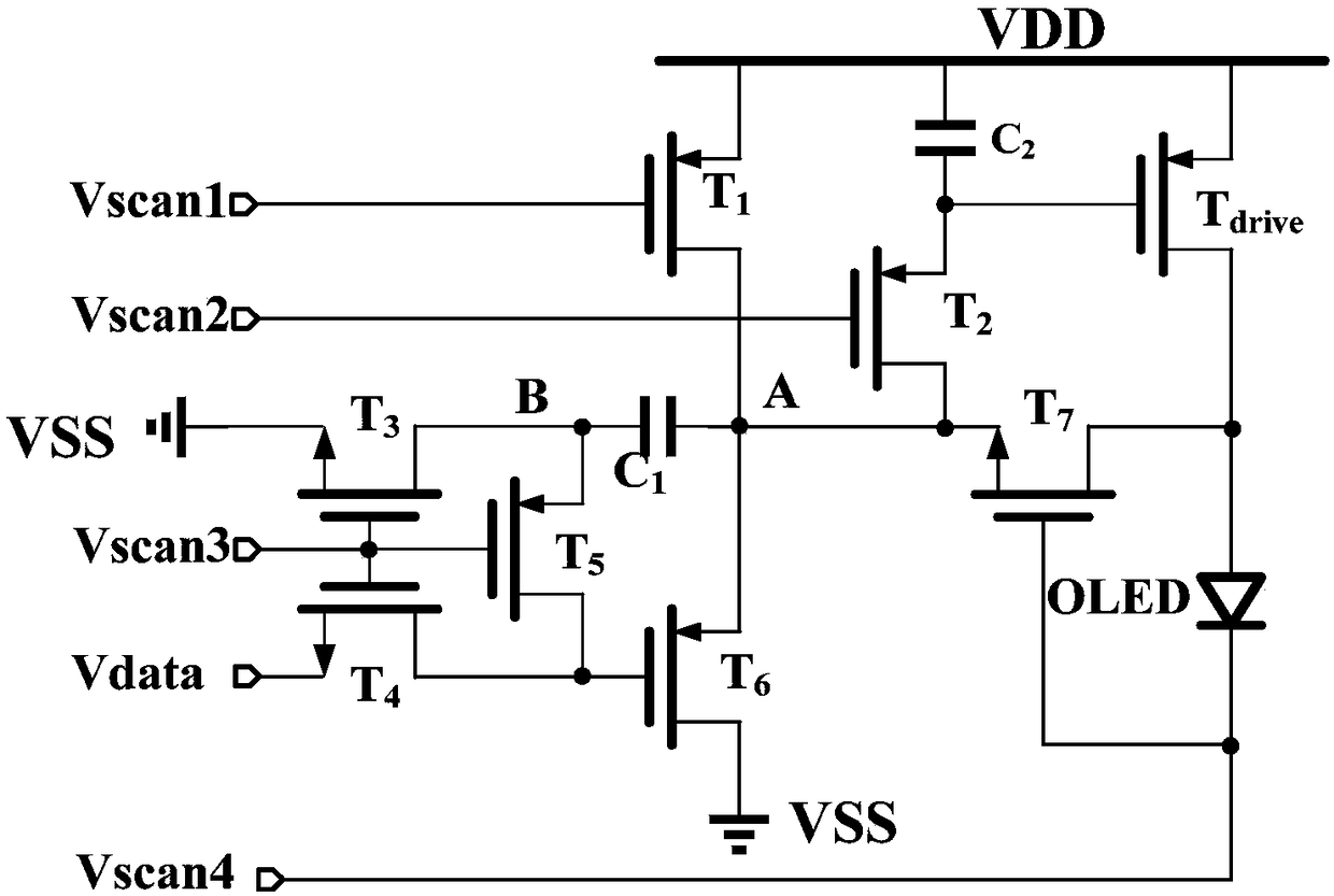
[0053] Such as image 3 As shown, this embodiment provides a voltage-programmable AMOLED pixel drive circuit, the drive circuit includes: a first switch transistor T1, a second switch transistor T2, a third switch transistor T3, a fourth switch transistor T4, a fifth switch transistor T5, sixth switching transistor T6, seventh switching transistor T7, driving transistor T drive , the first capacitor C1, the second capacitor C2 and the organic light-emitting diode OLED, referred to as 8T2C circuit. The first capacitor C1 and the second capacitor C2 are storage capacitors.
[0054] The first electrode of the first switching transistor T1 is connected to the power supply voltage, the second electrode is connected to the second electrode of the second switching transistor T2, the first electrode of the sixth switching transistor T6, and the seventh switching transistor T7 The first electrode of the first electrode and the first terminal and gate of the first capacitor C1 are con...
Embodiment 2
[0063] Such as Figure 3 ~ Figure 8 As shown, according to Embodiment 1, the driving method of the voltage-programmable AMOLED pixel circuit provided in this embodiment includes a pre-charging stage, a threshold voltage detection stage, a programming stage, and a light-emitting stage. The specific introduction is as follows:
[0064] Precharge phase: as Figure 4 As shown, the first control signal Vscan1 and the second control signal Vscan2 input low level, the third control signal Vscan3 and the fourth control signal Vscan4 input high level, so that the first switching transistor T1, the second switching transistor T2, the third switching transistor T1 The switch transistor T3, the fourth switch transistor T4, and the seventh switch transistor T7 are turned on, and the fifth switch transistor T5 is turned off. Since the fourth control signal Vscan4 is at a high level, the organic light emitting diode OLED is in a reverse-biased state that does not emit light. This reverse bi...
PUM
 Abstract
Description
Claims
Application Information
 - R&D
- Intellectual Property
- Life Sciences
- Materials
- Tech Scout
- Unparalleled Data Quality
- Higher Quality Content
- 60% Fewer Hallucinations
Browse by: Latest US Patents, China's latest patents, Technical Efficacy Thesaurus, Application Domain, Technology Topic, Popular Technical Reports.
© 2025 PatSnap. All rights reserved.Legal|Privacy policy|Modern Slavery Act Transparency Statement|Sitemap|About US| Contact US: help@patsnap.com


