Method of forming semiconductor structure

A semiconductor and logic transistor technology, applied in the field of semiconductor structure formation, can solve problems such as poor performance and inability to meet the development needs of semiconductor devices, and achieve the effect of improving performance

Active Publication Date: 2016-10-05
SEMICON MFG INT (SHANGHAI) CORP
View PDF3 Cites 1 Cited by
  • Summary
  • Abstract
  • Description
  • Claims
  • Application Information

AI Technical Summary

Problems solved by technology

[0019] However, semiconductor devices with split-gate flash memory, high-threshold voltage transistors, and logic transistors formed by existing technologies have poor performance and cannot meet the development needs of semiconductor devices.

Method used


Image

  • Method of forming semiconductor structure
  • Method of forming semiconductor structure
  • Method of forming semiconductor structure

Examples


Embodiment Construction

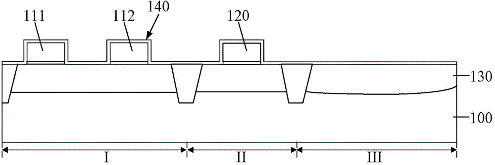
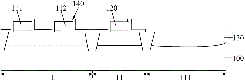
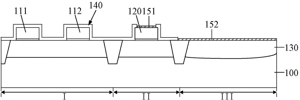
[0051] As mentioned in the background technology, semiconductor devices with split-gate flash memory, high threshold voltage transistors, and logic transistors formed by existing processes have poor performance, and the reasons for this are analyzed:

[0052] combined reference Figure 5 to Figure 8 , before forming the BARC layer 170, in the memory region I, the height of the first polysilicon layer 162 protruding from the semiconductor substrate 100 is equal to the height of the first gate layer 120 and the first polysilicon layer The sum of the thicknesses of the crystal silicon layer 162, and the height of the third polysilicon layer 163 in the logic device region III is only its own thickness (also equivalent to the thickness of the first polysilicon layer 162), so that the third polysilicon layer The height of the third polysilicon layer 163 is much lower than that of the first polysilicon layer 162 . In the prior art, the BARC layer 170 formation process is a spin-coat...


PUM


Abstract

The invention provides a method of forming a semiconductor structure, comprising the following steps: providing a semiconductor structure which comprises a first region and a second region arranged in parallel, wherein the first region and the second region are respectively used to form a first device and a logic transistor; forming a first gate layer on the first region, and forming a first insulating layer on the first gate layer; forming a first semiconductor layer on the first gate layer, and forming an anti-reflection coating by spin coating after a second semiconductor layer is formed on the semiconductor substrate in the second region, wherein the thickness of the anti-reflection coating on the first semiconductor layer is smaller than that of the anti-reflection coating on the second semiconductor layer; etching the anti-reflection coating, the first semiconductor layer and the second semiconductor layer, forming a through hole exposing the first insulating layer in the first semiconductor layer, and forming a logic gate layer on the second region; and removing the first insulating layer at the bottom of the through hole to expose the first gate layer. By adopting the technical scheme, the performance of a semiconductor device formed subsequently can be improved.

Description

technical field [0001] The invention relates to the technical field of semiconductor manufacturing, in particular to a method for forming a semiconductor structure. Background technique [0002] Split-gate flash memory is a common type of non-volatile flash memory. Split-gate flash memory has become the mainstream technology of embedded memory devices with no over-erasing effect, relatively simple circuit design, and low-voltage, high-speed operation characteristics, and is widely used in electronic devices such as smart cards, SIM cards, microcontrollers, and mobile phones. product. [0003] In the existing manufacturing process of split-gate flash memory, a peripheral circuit (Periphery Circuit) is usually arranged around the split-gate flash memory. The peripheral circuit is mainly a logic circuit, including: a high threshold voltage transistor and a logic transistor. The logic circuit is used to introduce different voltages to control the split-gate flash memory to pe...

Claims


Application Information

Patent Timeline
Patent Type & Authority Applications(China)
IPC IPC(8): H01L21/8247H10B41/35
Inventor 杨震
Owner SEMICON MFG INT (SHANGHAI) CORP
Why Eureka
Try Eureka