Laminated wiring film for electronic components and sputtering target for coating layer formation
A technology for laminating wiring films and electronic components, which is applied in sputtering plating, ion implantation plating, coating, etc., can solve the problems of easy peeling and low adhesion, improve reliability, and facilitate stable manufacturing Effect
- Summary
- Abstract
- Description
- Claims
- Application Information
AI Technical Summary
Problems solved by technology
Method used
Image
Examples
Embodiment 1
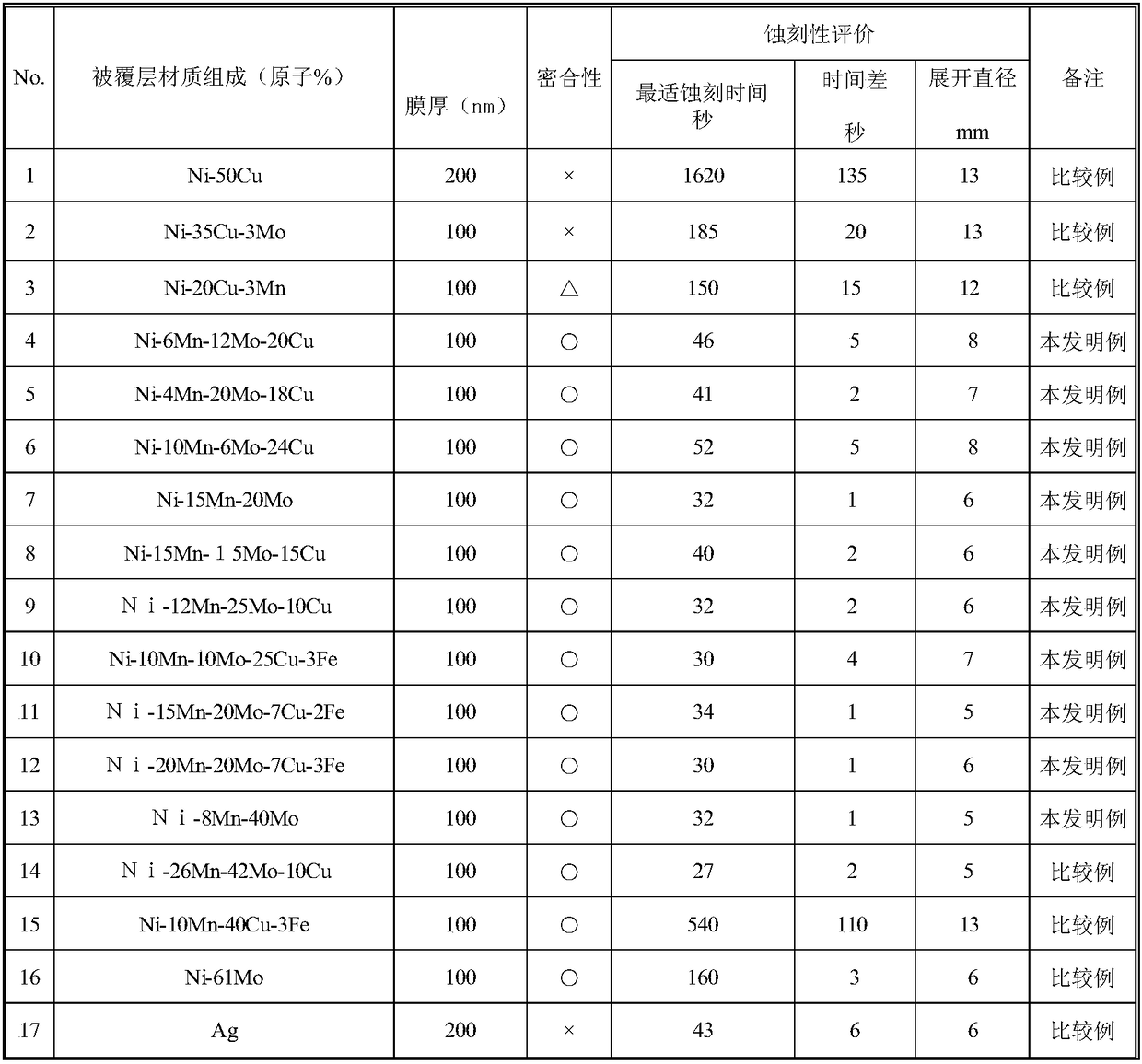
[0076] First, the sputtering targets for coating layer formation of sample No. 1-12 and sample No. 14 shown in Table 1 were prepared. Using the vacuum melting method, the raw materials are weighed so as to form each composition, and an ingot is produced by melting and casting in a vacuum melting furnace. The ingot was machined without plastic working, and a sputtering target with a diameter of 100 mm and a thickness of 5 mm was produced. Moreover, the sputtering target material of Ni-16 atomic % Mn was also produced by the same method.
[0077] In addition, Mo powder with a purity of 99.99%, an average particle size of 6 μm, and a powder of Ni with an average particle size of 70 μm were weighed, mixed with a cross rotary mixer to obtain a mixed powder, and then filled into a soft container with an inner diameter of 133 mm, an outer diameter of 139 mm, and a height of 30 mm. in a steel container. Then, the mild steel container was heated at 450° C. for 10 hours, degassed, sea...
Embodiment 2
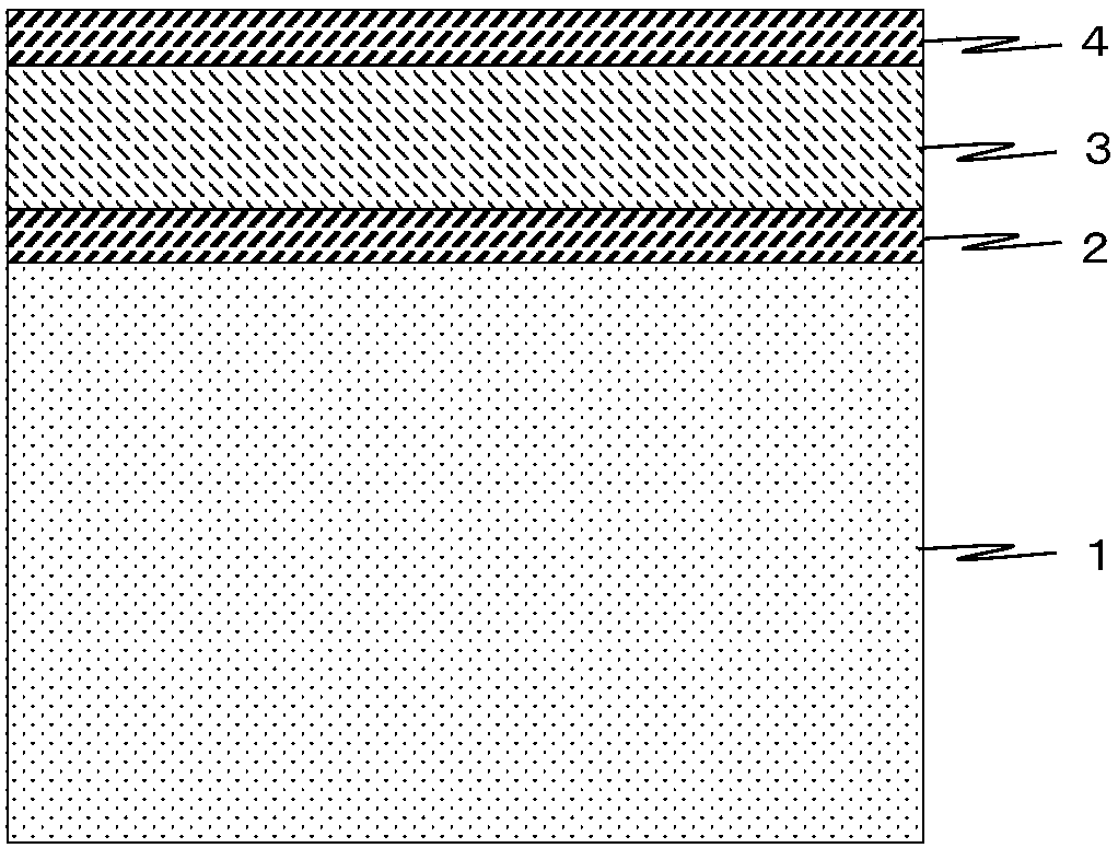
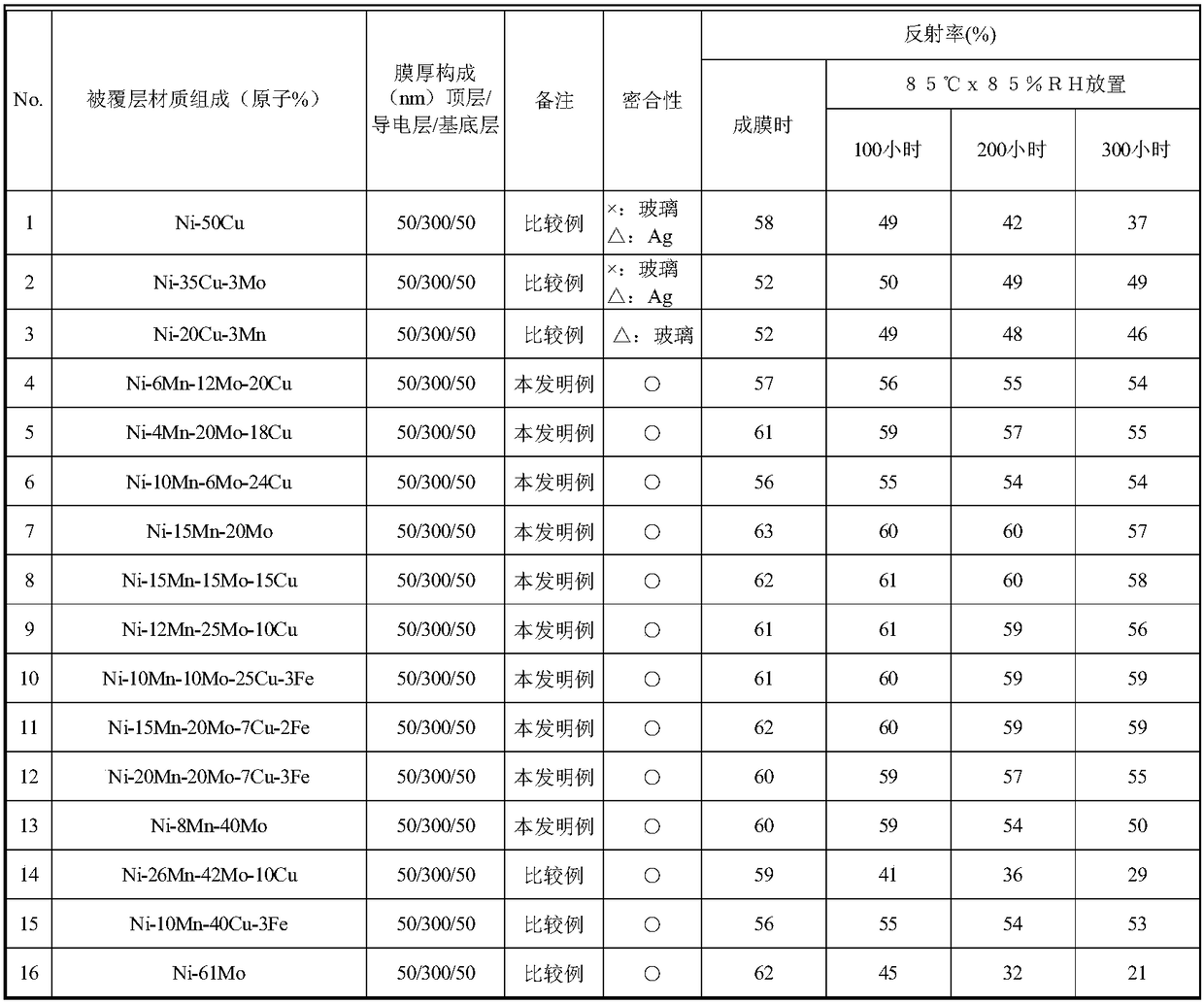
[0093] Using each sputtering target produced in Example 1, a laminated wiring film in which an underlayer with a film thickness of 50 nm, a conductive layer made of Ag with a film thickness of 200 nm, and a top layer with a film thickness of 50 nm was sequentially formed on a glass substrate was produced. sample. Furthermore, the adhesiveness of each sample and the moisture resistance which is one of weather resistance were evaluated. It should be noted that the above-mentioned base layer and top layer are layers composed of the covering layer materials in Table 2.
[0094] Adhesive evaluation was performed by the method similar to Example 1. Then, the case where one piece was not peeled off was evaluated as ◯, the case where 1 to 10 pieces were peeled was evaluated as Δ, and the case where 11 or more pieces were peeled was evaluated as x.
[0095] In addition, in the evaluation of moisture resistance, the prepared laminated wiring film was left to stand in an atmosphere at ...
Embodiment 3
[0103] Oxidation resistance was evaluated using samples of the laminated wiring film produced in Example 2. Each sample was heat-processed at the temperature of 200 degreeC - 300 degreeC for 30 minutes in air atmosphere, and it measured reflectance similarly to Example 2. Table 3 shows the evaluation results.
[0104] [table 3]
[0105]
[0106] On a film substrate, oxidation resistance up to 250°C is required. As shown in Table 3, it was confirmed that, in sample No.1 to sample No.3 and No.14 which are comparative examples, the reflectance starts to decrease at 250° C. or higher.
[0107] On the other hand, it turns out that the laminated wiring film for electronic components of this invention maintains the high reflectance of 50% or more up to 250 degreeC, and has high oxidation resistance. Furthermore, at a high temperature of 300°C, for samples No. 6 and No. 10 in which the total amount of Mn and Cu exceeds 30%, the reflectance decreases. Therefore, in order to obtai...
PUM
 Abstract
Description
Claims
Application Information
 - Generate Ideas
- Intellectual Property
- Life Sciences
- Materials
- Tech Scout
- Unparalleled Data Quality
- Higher Quality Content
- 60% Fewer Hallucinations
Browse by: Latest US Patents, China's latest patents, Technical Efficacy Thesaurus, Application Domain, Technology Topic, Popular Technical Reports.
© 2025 PatSnap. All rights reserved.Legal|Privacy policy|Modern Slavery Act Transparency Statement|Sitemap|About US| Contact US: help@patsnap.com


