Frame, diode comprising same and processing technology of diode
A diode and frame technology, applied in the field of photovoltaic equipment, to achieve the effect of ensuring heat dissipation efficiency, improving electrical performance, and optimal use stability
- Summary
- Abstract
- Description
- Claims
- Application Information
AI Technical Summary
Problems solved by technology
Method used
Image
Examples
Embodiment Construction
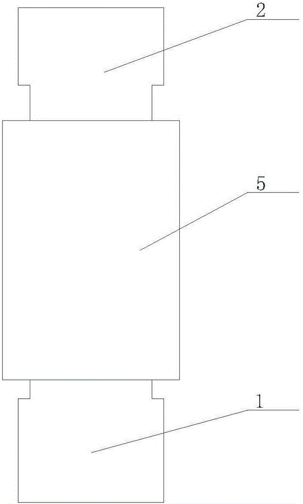
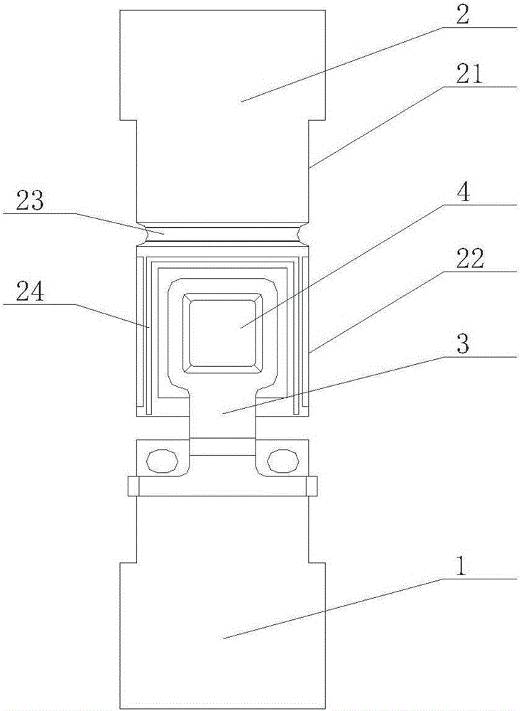
[0038] The invention is like Figure 1-11 As shown, it includes a positive plate 1 for connecting a jumper 3 and a negative plate 2 for connecting a chip 4;
[0039] The negative plate 2 includes a wiring board 21 and a chip board 22 that are connected as a whole. A groove 23 is formed between the wiring board 21 and the chip board 22, and the cross section of the groove 23 is small in the bottom and large in the top. ;
[0040] The chip board 22 has a chip area for supporting the chip 4, the outer side of the chip area is provided with a groove 24, the outer edge of the chip board 22 is stepped, and the outer side of the chip board 22 is facing Depressed inside.
[0041] The thickness of the positive electrode plate 1 and the negative electrode plate 2 are both less than 0.6 mm. In this case, the finished product and heat transfer efficiency were fully considered, and the thickness of the positive and negative plates was greatly reduced (to less than half of the existing technolo...
PUM
 Abstract
Description
Claims
Application Information
 - R&D
- Intellectual Property
- Life Sciences
- Materials
- Tech Scout
- Unparalleled Data Quality
- Higher Quality Content
- 60% Fewer Hallucinations
Browse by: Latest US Patents, China's latest patents, Technical Efficacy Thesaurus, Application Domain, Technology Topic, Popular Technical Reports.
© 2025 PatSnap. All rights reserved.Legal|Privacy policy|Modern Slavery Act Transparency Statement|Sitemap|About US| Contact US: help@patsnap.com


