
Halftone mask plate and fabrication method of thin film transistor (TFT) substrate

A half-tone mask and substrate technology, which is applied in the photoengraving process of the pattern surface, the manufacture of semiconductor/solid-state devices, the originals for optical mechanical processing, etc. problems such as low rate, to avoid over-display and over-engraving, and eliminate insufficient yield rate

Active Publication Date: 2016-08-24
SHENZHEN CHINA STAR OPTOELECTRONICS TECH CO LTD
View PDF3 Cites 5 Cited by
  • Summary
  • Abstract
  • Description
  • Claims
  • Application Information

AI Technical Summary

Problems solved by technology

[0012] When the electrode, and the channel area produce edge effects, resulting in over-display and over-recording, so as to eliminate the problems of insufficient yield and low yield in the prior art
[0013] The object of the present invention is also to provide a method for manufacturing a TFT substrate. By using the above-mentioned half-tone mask, it is possible to avoid over-display and over-engraving caused by edge effects when the channel region is formed by patterning, thereby eliminating the problem of the yield rate in the prior art. Insufficient and low yield problems

Method used


Image

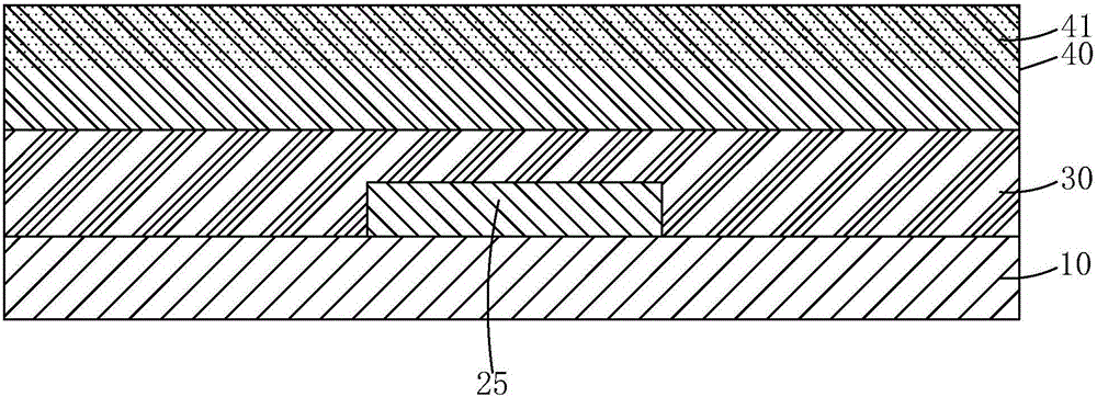
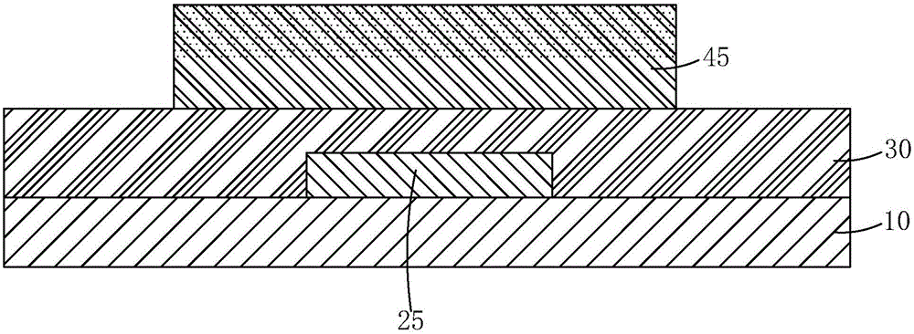
  • Halftone mask plate and fabrication method of thin film transistor (TFT) substrate
  • Halftone mask plate and fabrication method of thin film transistor (TFT) substrate
  • Halftone mask plate and fabrication method of thin film transistor (TFT) substrate

Examples


Embodiment Construction

[0058] In order to further illustrate the technical means adopted by the present invention and its effects, the following describes in detail in conjunction with preferred embodiments of the present invention and accompanying drawings.

[0059] see Figure 9 , the present invention firstly provides a half-tone mask, including first and second opaque regions 910, 920 corresponding to the positions of the source and drain of the thin film transistor, and used for the active area of ​​the thin film transistor. The U-shaped semi-transparent region 930 corresponding to the position of the U-shaped channel region of the layer, the two semi-transparent extension regions 940 located at the opening of the U-shaped semi-transparent region 930 and extending out of the opening, and the remaining full Light-transmitting region 950 .

[0060] Specifically, the first opaque area 910 includes a bar-shaped portion 911, the second opaque area 920 includes a U-shaped portion 921, and one end of...


PUM


Abstract

The invention provides a halftone mask and a fabrication method of a thin film transistor (TFT) substrate. The halftone mask comprises a first light-proof region, a second light-proof region, a U-shaped semi-transparent region, two semi-transparent extension regions and a remaining all-transparent region, wherein the first light-proof region and the second light-proof region are used for being in correspondence to a source position and a drain position of a TFT respectively, the U-shaped semi-transparent region is used for being in correspondence to a U-shaped channel region position of an active layer of the TFT, the two semi-transparent extension regions are located at an opening of the U-shaped semi-transparent region and extend towards the outside of the opening, and a fringe effect can be prevented from being generated to cause over-development and over-etching in the semi-transparent extension regions when a source region, a drain region and a channel region are formed through composition, so that the problems of low yield and too low production rate in the prior art are eliminated. According to the fabrication method of the TFT substrate, provided by the invention, the halftone mask plate is adopted, and the fringe effect can be prevented from being generated to cause over-development and over-etching when the channel region is formed through composition, so that the problems of low yield and too low production rate in the prior art are eliminated.

Description

technical field [0001] The invention relates to the field of display technology, in particular to a method for manufacturing a halftone mask and a TFT substrate. Background technique [0002] Liquid crystal displays are widely used in various daily necessities and office supplies, such as computers, mobile phones, and bulletin boards, due to their advantages of low energy consumption, low radiation, light weight, and thinness. [0003] The liquid crystal display includes a thin film transistor (Thin Film Transist, TFT) array substrate, a color filter substrate, and a liquid crystal layer injected between the two plates. When manufacturing a thin film transistor substrate, it is usually produced through 4 to 6 rounds of mask (Mask) processes, such as thin film deposition, mask exposure, development, and etching. With the development of science and technology, the emergence of half-tone masks has reduced the manufacturing process of LCD panels to 4Mask process technology. ...

Claims


Application Information

Patent Timeline
Patent Type & Authority Applications(China)
IPC IPC(8): G03F1/32H01L21/77
Inventor 莫超德
Owner SHENZHEN CHINA STAR OPTOELECTRONICS TECH CO LTD
Learn More