
Chip positioning device and chip positioning method

A technology of positioning device and positioning method, which is applied in the fields of fixed capacitor parts, fixed capacitor dielectric, capacitor manufacturing, etc., and can solve the problems of low chip termination efficiency, wrong chip positioning and orientation, etc.

Active Publication Date: 2018-06-26
GUANGDONG FENGHUA ADVANCED TECH HLDG
View PDF3 Cites 1 Cited by
  • Summary
  • Abstract
  • Description
  • Claims
  • Application Information

AI Technical Summary

Problems solved by technology

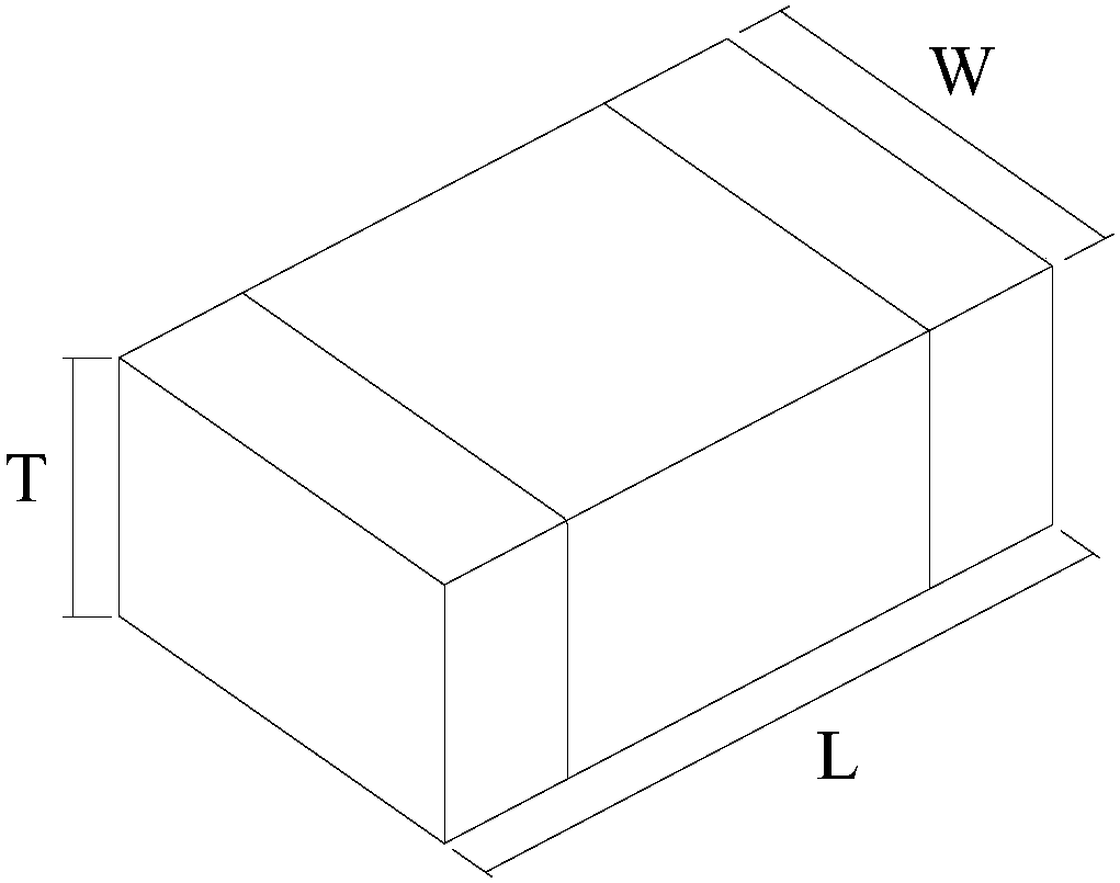
[0004] However, when the chip of the flip-chip multilayer ceramic capacitor is introduced into the plate hole of the terminal board, the problem of wrong orientation of the chip is prone to occur, so that the terminal electrodes are mistakenly formed on the two opposite short sides of the chip, so the flip-chip Type multilayer ceramic capacitors have low chip termination efficiency

Method used


Image

  • Chip positioning device and chip positioning method
  • Chip positioning device and chip positioning method
  • Chip positioning device and chip positioning method

Examples


Embodiment Construction

[0036] The chip positioning device and the chip positioning method used for the terminal sealing positioning of the chip of the flip-chip multilayer ceramic capacitor will be further described in detail below mainly in conjunction with the accompanying drawings and specific embodiments.

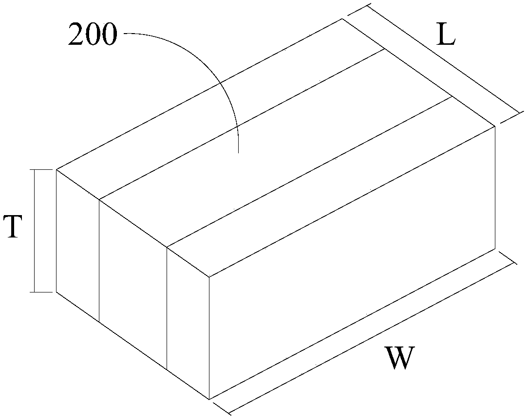
[0037] to combine figure 2 , the surface formed by the length (L) and width (W) of the chip 200 of the flip-chip multilayer ceramic capacitor is the main surface, and the surface formed by the length (L) and thickness (T) of the chip 200 is the short side, and the surface of the chip 200 The surfaces formed by width (W) and thickness (T) are long sides. Terminal electrodes of the flip-chip multilayer ceramic capacitor are formed on opposite long sides of the chip 200 .

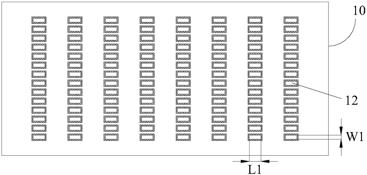
[0038] to combine Figure 3 ~ Figure 4 , the chip positioning device of an embodiment used for the termination positioning of the chip 200 of the flip-chip multilayer ceramic capacitor includes: a first guide plate 10 , a ...


PUM


Abstract

The invention discloses a chip positioning device and a chip positioning method. The chip positioning device is used for end encapsulation positioning of the chips of inverted type multi-layer ceramic capacitors. The chip positioning device includes a first guide plate with a plurality of uniformly-arranged first through holes, a second guide plate with a plurality of uniformly-arranged second through holes, and a positioning plate with a plurality of uniformly-arranged third through holes; the length and width of the first through holes are matched with the length and thickness of the chips; the number and distribution positions of the second through holes are matched with the number and distribution positions of the first through holes; the width of the second through holes is equal to the width of the first through holes; the depth of the second through holes is larger than the width of the chips; the number and the distribution positions of the third through holes are matched with the number and the distribution positions of the second through holes; and the width of the third through holes is equal to the width of the second through holes. With the chip positioning device and the chip positioning method adopted, the orientation of the positioning of the chips of the inverted type multi-layer ceramic capacitors in end encapsulation can be ensured, end encapsulation efficiency can be improved, and operation is convenient.

Description

technical field [0001] The invention relates to the field of electronic components, in particular to a chip positioning device and a chip positioning method for end-sealing positioning of chips of flip-chip multilayer ceramic capacitors. Background technique [0002] Flip-chip multilayer ceramic capacitors are a kind of specially designed multilayer ceramic capacitors. The specifications include 0204, 0306, 0508, 0612, etc. The difference from conventional multilayer ceramic capacitors is that the length and width of the capacitor chip are reversed. For example, the flip-chip multilayer ceramic capacitor corresponding to the 0402 specification (0.04 inches in length and 0.02 inches in width) of a conventional multilayer ceramic capacitor is the 0204 specification (0.02 inches in length and 0.04 inches in width). The flip-chip multilayer ceramic capacitor has a greatly reduced aspect ratio compared with conventional products, so the equivalent series inductance is greatly red...

Claims


Application Information

Patent Timeline
Patent Type & Authority Patents(China)
IPC IPC(8): H01G13/00H01G4/30H01G4/12
CPCH01G4/12H01G4/30H01G13/00
Inventor 陆亨廖庆文安可荣卓金丽
Owner GUANGDONG FENGHUA ADVANCED TECH HLDG
Learn More