A display substrate and its manufacturing method

A manufacturing method and technology for display substrates, which are applied in the manufacture of semiconductor/solid-state devices, instruments, electrical components, etc., can solve problems such as defects in metal wire grids, and achieve the effect of ensuring the accuracy of splicing

Inactive Publication Date: 2019-03-22
BOE TECH GRP CO LTD
View PDF4 Cites 0 Cited by
  • Summary
  • Abstract
  • Description
  • Claims
  • Application Information

AI Technical Summary

Problems solved by technology

[0004] The purpose of the present invention is to provide a display substrate and its manufacturing method to solve the technical problem that the spliced ​​metal wire grids on the existing large-size substrate often have defects

Method used


Image

  • A display substrate and its manufacturing method
  • A display substrate and its manufacturing method
  • A display substrate and its manufacturing method

Examples


Embodiment Construction

[0043] The following will clearly and completely describe the technical solutions in the embodiments of the present invention with reference to the accompanying drawings in the embodiments of the present invention. Obviously, the described embodiments are some of the embodiments of the present invention, but not all of them. Based on the embodiments of the present invention, all other embodiments obtained by persons of ordinary skill in the art without creative efforts fall within the protection scope of the present invention.

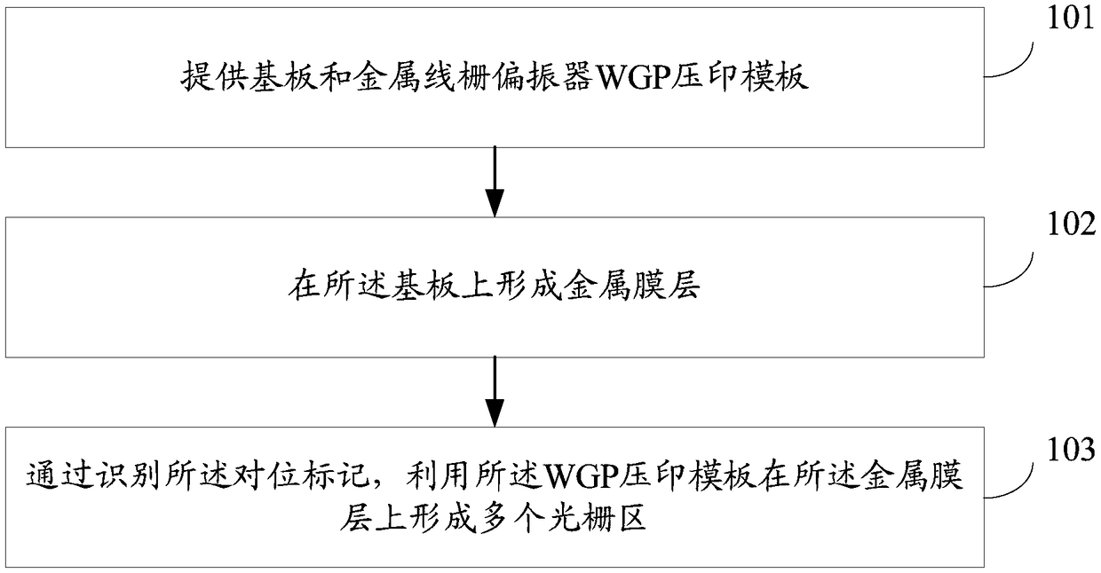
[0044] see figure 1 As shown, the embodiment of the present invention provides a method for manufacturing a display substrate, including the following steps:

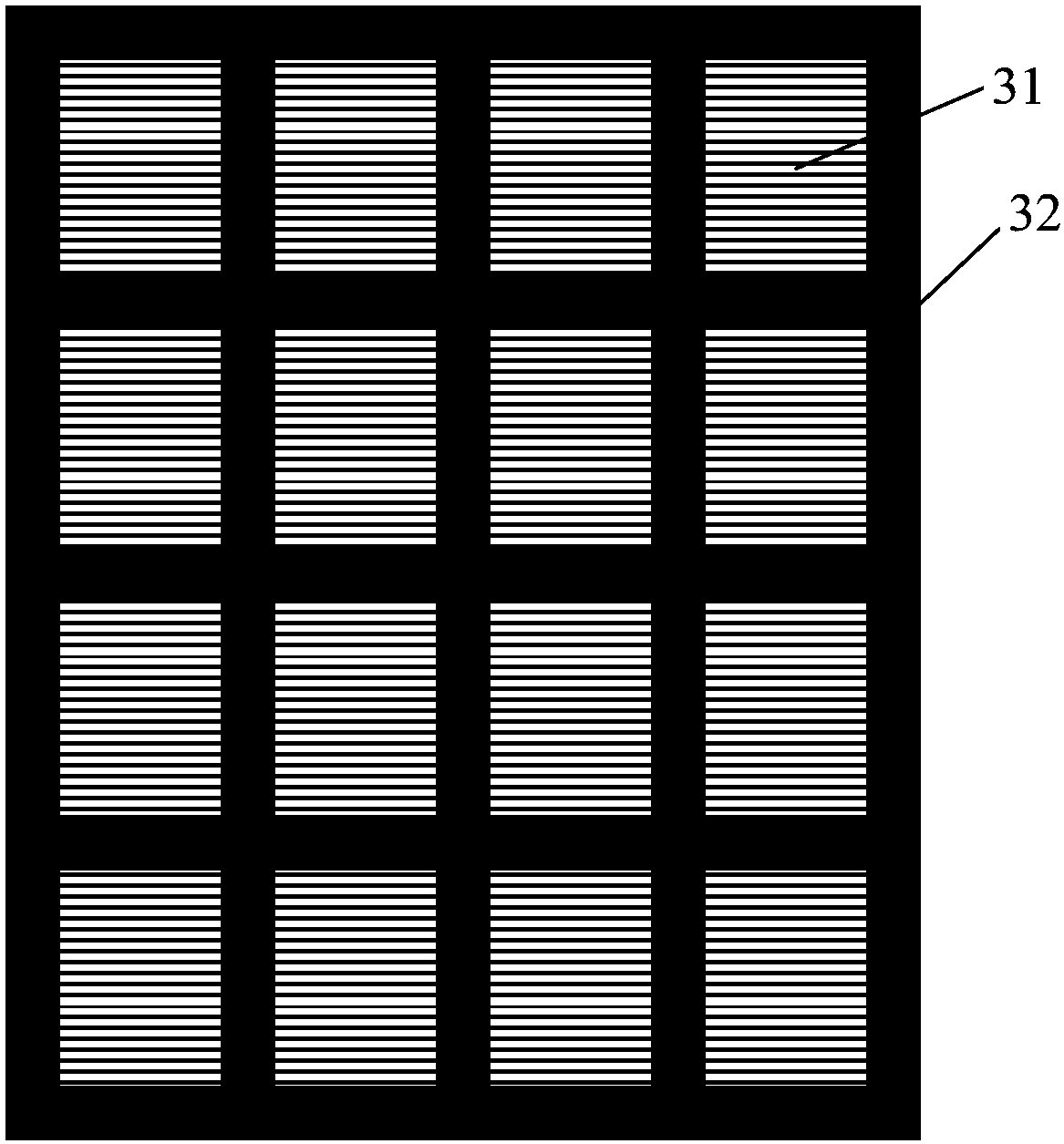
[0045] Step 101: providing a substrate and a metal wire grid polarizer WGP imprint template, the substrate has an alignment mark in a non-pixel area, and the size of the display area of ​​the substrate is larger than the size of the WGP imprint template;

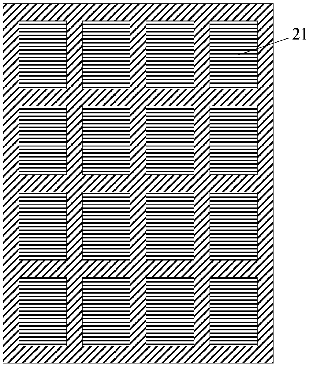
[0046] Step 102: forming a metal film ...


PUM

PropertyMeasurementUnit
thicknessaaaaaaaaaa

Abstract

The invention provides a display substrate and a manufacturing method thereof. The manufacturing method comprises the steps that a substrate and a metal wire gating polarizer WGP imprinting template are provided, alignment marks positioned in a non-pixel region are positioned on the substrate, a metal film layer is formed on the substrate, a plurality of grating regions are formed on the metal film layer through recognizing the alignment marks and utilizing the WGP imprinting template, one of the grating region is formed through one-time imprinting of the WGP imprinting template, and a splicing position of the adjacent grating regions is positioned in the non-pixel region. The manufacturing method provided by the invention can be used for forming the grating regions on the metal film layer of the substrate through recognizing the alignment marks in the non-pixel region, so that the splicing position of the adjacent grating regions is positioned in the non-pixel region, thereby ensuring splicing precision, and preventing defects occurred in spliced gratings from affecting the subsequent display content.

Description

technical field [0001] The invention relates to the field of display technology, in particular to a display substrate and a manufacturing method thereof. Background technique [0002] A wire grid polarizer (WGP for short) is composed of parallel metal wires, the metal wires have a nanoscale cross-section and a macroscopic length, and are capable of polarizing light. In order to reduce the thickness of the device, the existing liquid crystal display device can use the metal wire grid integrated on the substrate to replace the polarizer attached to the substrate to improve product performance. [0003] Specifically, the preparation of the metal wire grid requires high-precision photolithography or nanoimprinting technology, but these technologies are difficult to prepare a large-sized WGP substrate with a complete metal wire grid. In order to prepare WGP on large-size substrates, splicing technology is usually used to form metal wire grids, but the existing splicing technolog...

Claims


Application Information

Patent Timeline
Patent Type & Authority Patents(China)
IPC IPC(8): H01L21/77G02F1/1333
CPCG02F1/1333H01L21/77
Inventor 关峰曹占锋姚琪
Owner BOE TECH GRP CO LTD
Why Eureka
Try Eureka