A chip temperature sensor and its preparation process
A technology of temperature sensor and preparation process, which is applied to thermometers, thermometers and instruments using electric/magnetic elements that are directly sensitive to heat, to achieve the effects of high measurement accuracy, stable measurement accuracy, and small volume
- Summary
- Abstract
- Description
- Claims
- Application Information
AI Technical Summary
Problems solved by technology
Method used
Image
Examples
no. 1 example
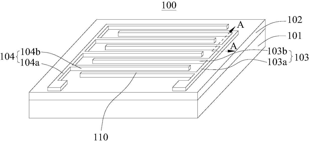
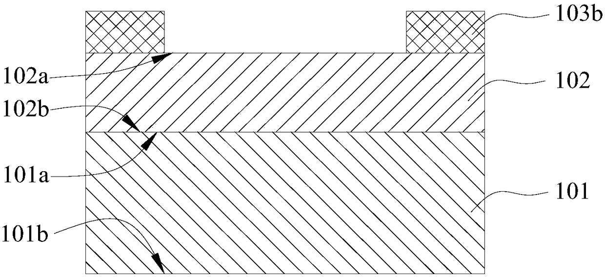
[0038] see figure 1 and figure 2As shown, this embodiment provides a chip-type temperature sensor 100, the temperature sensor 100 is in the form of a sheet, the length and width of the temperature sensor 100 are not greater than 1 mm, the thickness of the temperature sensor 100 is not greater than 550 μm, and the temperature sensor 100 is in the form of a sheet Structure, and small size, so it can be directly attached to any part of the surface of the object to be measured, used to measure the local temperature of the surface of the object, and the surface temperature of objects of different shapes. The temperature sensor 100 includes a substrate 101 , a germanium film (Ge film) 102 , and interdigital electrodes 110 . The germanium film 102 is a temperature-sensitive material and is the core part of the temperature sensor 100. The germanium film 102 is located on the first surface 101a (ie, the upper surface) of the substrate 101. The germanium film 102 has a second surface ...
no. 2 example
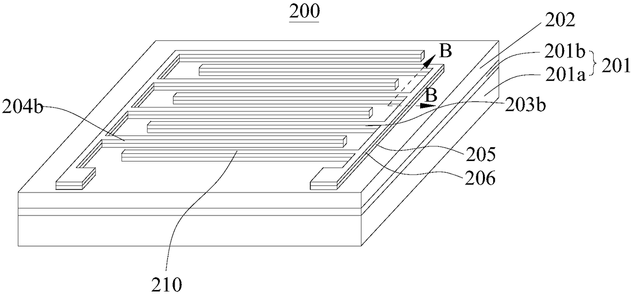
[0050] see image 3 and Figure 4 As shown, the provided chip temperature sensor 200 has substantially the same structure as the chip temperature sensor 100 provided in the first embodiment. The temperature sensor 200 includes a substrate 201 , a germanium film 202 , and interdigital electrodes 210 . The germanium film 202 is located on the first surface 201c of the substrate 201 , and the interdigital electrodes 210 are located on the second surface 202a of the germanium film 202 .
[0051] The difference between the two is that in this embodiment, the substrate 201 is single crystal silicon with an oxide layer, the substrate 201 includes a silicon layer 201a and a silicon oxide layer 201b stacked from bottom to top, and the thickness of the silicon layer 201a is 300-500 μm. The thickness of the silicon oxide layer 201b is 0.2-0.4 μm. Preferably, the thickness of the silicon layer 201 a is 500 μm, the thickness of the silicon oxide layer 201 b is 0.4 μm; the thickness of th...
no. 3 example
[0057] see Figure 5 As shown, the structure of the chip temperature sensor 200a provided in this embodiment is substantially the same as that of the chip temperature sensor 200 provided in the second embodiment, the difference between the two is that in this embodiment, the thickness of the silicon layer 201a is 400 μm , the thickness of the silicon oxide layer 201b is 0.3 μm. The germanium film 202 has a thickness of 1 μm.
[0058] The interdigital electrode 210 includes a titanium layer 205 and a gold layer 206 stacked from bottom to top. The thickness of the titanium layer 205 is 0.03 μm, and the thickness of the gold layer 206 is 0.2 μm. The interdigital width of the interdigital electrode 210=interdigital Pitch = 5 μm. The Ti / Au electrode of the thin film is an interdigitated structure, and the interdigital width and interdigital spacing are both 5um. The reason for doing this is that the germanium film 202 is an intrinsic semiconductor, and its resistance is very lar...
PUM
| Property | Measurement | Unit |
|---|---|---|
| width | aaaaa | aaaaa |
| thickness | aaaaa | aaaaa |
| thickness | aaaaa | aaaaa |
Abstract
Description
Claims
Application Information
 - R&D
- Intellectual Property
- Life Sciences
- Materials
- Tech Scout
- Unparalleled Data Quality
- Higher Quality Content
- 60% Fewer Hallucinations
Browse by: Latest US Patents, China's latest patents, Technical Efficacy Thesaurus, Application Domain, Technology Topic, Popular Technical Reports.
© 2025 PatSnap. All rights reserved.Legal|Privacy policy|Modern Slavery Act Transparency Statement|Sitemap|About US| Contact US: help@patsnap.com


