
Array substrate as well as display panel with same and display device with same

A technology for array substrates and display panels, applied in instruments, nonlinear optics, optics, etc., can solve problems such as liquid crystal display panel smearing, liquid crystal molecule rotation disorder, and synthetic electric field disorder, so as to improve display effects and improve smearing The effect of the phenomenon

Active Publication Date: 2016-07-06
XIAMEN TIANMA MICRO ELECTRONICS +1
View PDF5 Cites 2 Cited by
  • Summary
  • Abstract
  • Description
  • Claims
  • Application Information

AI Technical Summary

Problems solved by technology

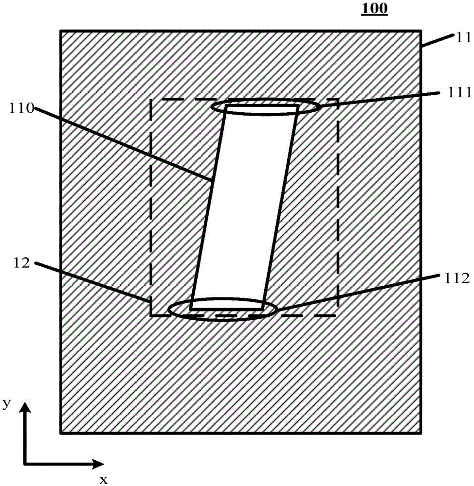
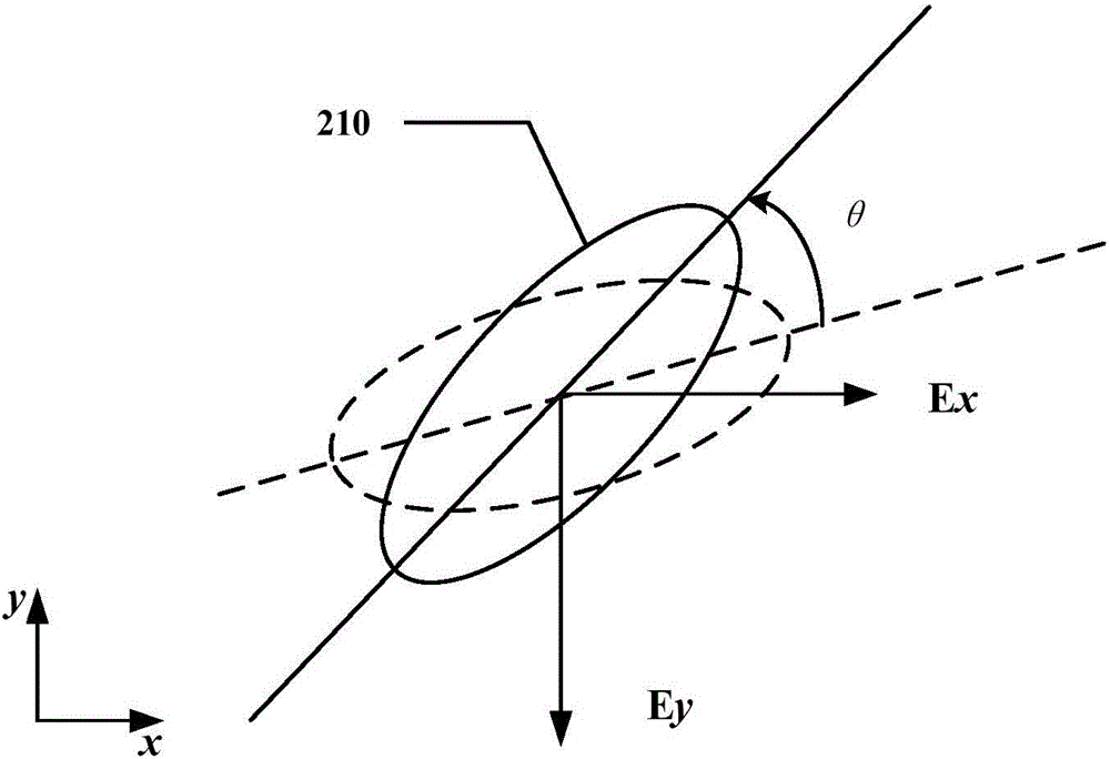
Due to the different distances and structures between the pixel electrodes and the common electrode 100, the components of Ex and Ey are also different in different regions at the end, resulting in disordered synthetic electric fields and disordered rotation of liquid crystal molecules.
At the same time, when an external force is applied to the liquid crystal display panel, the liquid crystal molecules near the end of the light-transmitting region 12 of the pixel, that is, at the two ends 111 and 112 of the strip-shaped opening, will be deflected under the action of the external force, thereby forming dark domain lines at this position. , and it is difficult to disappear for a long period of time after the external force is withdrawn, which makes the tailing phenomenon of the LCD panel serious and affects the display effect

Method used


Image

  • Array substrate as well as display panel with same and display device with same
  • Array substrate as well as display panel with same and display device with same
  • Array substrate as well as display panel with same and display device with same

Examples


Embodiment Construction

[0026] The application will be further described in detail below in conjunction with the accompanying drawings and embodiments. It should be understood that the specific embodiments described here are only used to explain related inventions, rather than to limit the invention. It should also be noted that, for ease of description, only parts related to the invention are shown in the drawings.

[0027] It should be noted that, in the case of no conflict, the embodiments in the present application and the features in the embodiments can be combined with each other. The present application will be described in detail below with reference to the accompanying drawings and embodiments.

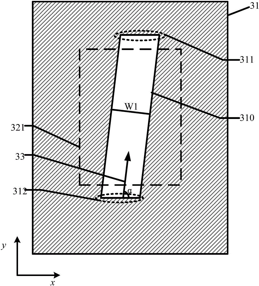
[0028] see Figure 3A Shown is a schematic structural view of the first electrode of an embodiment in the array substrate of the present application.

[0029] In this embodiment, the array substrate includes a base substrate, a plurality of scanning lines and a plurality of data lines arranged cr...


PUM

PropertyMeasurementUnit
Widthaaaaaaaaaa
Widthaaaaaaaaaa

Abstract

The invention discloses an array substrate as well as a display panel with the same and a display device with the same. The array substrate comprises a lining substrate, a plurality of pixel units, first electrodes and second electrodes, wherein the plurality of pixel units are arranged on the lining substrate; the first electrodes and the second electrodes are arranged inside the pixel units; the first electrodes are arranged on the second electrodes; the first electrodes comprise first stripy opening areas which extend in a first direction; the first opening areas comprise first ends and second ends; orthographic projection of photic zones of the pixel units to the plane of the lining substrate covers a part of the first opening areas between the first ends and the second ends; orthographic projection of non-photic zones of the pixel units to the plane of the lining substrate covers orthographic projection of the first ends and the second ends to the plane of the lining substrate. Therefore, in a formed electric field, electric field components which result in disordered twisting of liquid crystal molecules are positioned in the non-photic zones of the pixel units, and thus the trailing phenomenon of the non-photic zones of the pixel units can be reduced.

Description

technical field [0001] The present disclosure generally relates to display technology, and in particular, to an array substrate, a display panel including the same, and a display device. Background technique [0002] A liquid crystal display panel generally includes an array substrate, a color filter substrate disposed opposite to the array substrate, and a liquid crystal layer formed between the array substrate and the color filter substrate. The array substrate includes a plurality of pixel regions arranged in an array, and a pixel electrode and a common electrode are formed in each pixel region. By applying different voltages to the pixel electrode and the common electrode, the liquid crystal molecules in the liquid crystal layer can be rotated accordingly, so that the display panel can display a predetermined picture. [0003] In some liquid crystal display panels in the prior art, the common electrode is disposed on the pixel electrode. Such as figure 1 As shown, the...

Claims


Application Information

Patent Timeline
IPC IPC(8): G02F1/1343
CPCG02F1/134309G02F1/134363G02F1/134318G02F1/134372G02F1/136222G02F1/133514G02F1/1337G02F1/134336G02F1/136286G02F1/1368
Inventor 马扬昭沈柏平吴玲
Owner XIAMEN TIANMA MICRO ELECTRONICS
Learn More