Touch scanning circuit, driving method thereof, touch driving circuit and touch display screen
A touch scanning and circuit technology, applied in the fields of touch scanning circuits, touch driving circuits and touch display screens, can solve the problems of increasing wiring space, limiting the application of embedded technology, and increasing the number of
- Summary
- Abstract
- Description
- Claims
- Application Information
AI Technical Summary
Problems solved by technology
Method used
Image
Examples
example 1
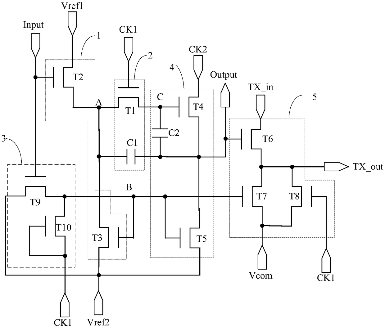
[0115] Figure 3a Take the touch scanning circuit shown as an example, and the corresponding input and output timing diagram is as follows Figure 5a shown. Specifically, choose the Figure 5a The four stages of T1 ~ T4 in the input and output sequence diagram shown.
[0116] In the T1 stage: Input=1, CK1=1, CK2=0.
[0117] Because Input=1, the second switch transistor T2 and the ninth switch transistor T9 are turned on, and because CK1=1, the first switch transistor T1, the tenth switch transistor T10 and the eighth switch transistor T8 are turned on; the second reference signal terminal Vref2 The low-potential signal of the first clock signal terminal CK1 is provided to the second node B through the turned-on ninth switch transistor T9, and the high-potential signal of the first clock signal terminal CK1 is provided to the second node B through the turned-on tenth switch transistor T10, so the second Node B is low potential, and the second node B of low potential control...
example 2
[0127] Figure 3b Take the touch scanning circuit shown as an example, and the corresponding input and output timing diagram is as follows Figure 5b shown. Specifically, choose the Figure 5b The four stages of T1 ~ T4 in the input and output sequence diagram shown.
[0128] In the T1 stage: Input=1, CK1=1, CK2=0.
[0129] Since Input=1, the second switch transistor T2 and the eleventh switch transistor T11 are turned on, and because CK1=1, the first switch transistor T1 and the eighth switch transistor T8 are turned on; the low potential signal of the second reference signal terminal Vref2 passes through The turned-on eleventh switching transistor T11 is provided to the second node B, and at the same time, the first clock signal terminal CK1 starts to charge the third capacitor C3, the potential of the second node B is a low potential, and the low potential second node B controls the second node B The three switching transistors T3, the fifth switching transistor T5 and ...
example 3
[0139] Figure 3c Take the touch scanning circuit shown as an example, and the corresponding input and output timing diagram is as follows Figure 5a shown. Specifically, choose the Figure 5a The four stages of T1 ~ T4 in the input and output sequence diagram shown.
[0140] In the T1 stage: Input=1, CK1=1, CK2=0.
[0141] Since Input=1, the second switching transistor T2, the twelfth switching transistor T12 and the thirteenth switching transistor T13 are turned on, and since CK1=1, the first switching transistor T1, the fourteenth switching transistor T14 and the eighth switching transistor T8 conduction; the low potential signal of the second reference signal terminal Vref2 is provided to the gate of the fifteenth switching transistor T15 through the turned-on twelfth switch transistor T12; the low potential signal of the second reference signal terminal Vref2 is passed through the turned-on first The thirteenth switch transistor T13 is provided to the second node B; a...
PUM
 Abstract
Description
Claims
Application Information
 - R&D
- Intellectual Property
- Life Sciences
- Materials
- Tech Scout
- Unparalleled Data Quality
- Higher Quality Content
- 60% Fewer Hallucinations
Browse by: Latest US Patents, China's latest patents, Technical Efficacy Thesaurus, Application Domain, Technology Topic, Popular Technical Reports.
© 2025 PatSnap. All rights reserved.Legal|Privacy policy|Modern Slavery Act Transparency Statement|Sitemap|About US| Contact US: help@patsnap.com


