
High-speed massive data storage system

A technology for massive data and storage systems, which is applied in electrical digital data processing, instruments, input/output to record carriers, etc. The effect of large capacity and strong scalability

Inactive Publication Date: 2016-06-01
JIANGSU LVYANG ELECTRONICS INSTR GROUP
View PDF4 Cites 3 Cited by
  • Summary
  • Abstract
  • Description
  • Claims
  • Application Information

AI Technical Summary

Problems solved by technology

The current mainstream Flash-based high-speed mass storage module generally uses the basic idea of ​​multi-chip parallelism to improve data storage speed, but its performance cannot meet the needs of some higher-speed data recording occasions, and many storage modules have external high-speed The interface is a dedicated non-standard interface, and the scalability and versatility are limited when building a storage system

Method used


Image

  • High-speed massive data storage system

Examples


Embodiment Construction

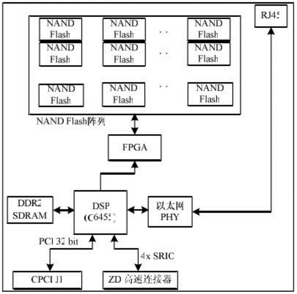
[0011] The physical structure of the storage module using NANDFlash as the storage medium adopts the standard CPCI6U board type, which is mainly composed of NANDFlash array, large-scale FPGA, high-performance DSP and various on-board connectors. Its structural block diagram is as follows: figure 1 shown. NANDFlash array and FPGA together constitute the core unit of the storage module. The NAND Flash array is composed of 96 high-density NAND Flash memory chips interconnected in groups, and its hardware is compatible with 2GB / 4GB / 8GB capacity memory chips, which can realize data storage spaces with a total capacity of 192GB, 384GB, and 768GB. Structurally, the 96 memory chips are extended in units of 8 to form a group, which is divided into 12 chip groups, and each of the 3 groups shares a data storage bus, forming a 4-way parallel bus structure. Large-scale FPGA mainly acts as a Flash array controller to perform control operations such as reading, writing and erasing data on e...


PUM


Abstract

The invention belongs to the field of digital signal processing, and discloses a high-speed massive data storage system. The system comprises an NAND Flash array, an FPGA, a DSP, an Ethernet PHY, a DDR2 SARAM, a CPCI J1 and a ZD high-speed connector, wherein the FPGA is electrically connected with each of the NAND Flash array and the DSP; the DSP communicates with each of the Ethernet PHY, the DDR2 SDRAM, the CPCI J1 and the ZD high-speed connector; the NAND Flash array adopts a spatial parallel and time parallel method to broaden the storage bandwidth; the DSP provides a standard high-speed interface for the DDR2 SDRAM and is connected with the FPGA through an EMIF bus; and the DSP receives an instruction from an external master control end and transmits the instruction to the FPGA. The system disclosed in the invention has favorable system expansibility and universality.

Description

technical field [0001] The invention belongs to the field of digital signal processing, in particular to a high-speed mass data storage system. Background technique [0002] Data acquisition and storage devices are widely used in radar, image processing, aviation and other fields. The rapid improvement of the performance of analog-to-digital conversion devices (ADC) has led to the rapid development of data acquisition technology, which puts higher demands on the capacity and bandwidth of data storage devices. In addition, the power consumption and volume of the storage device are also important considerations. Disk-based storage devices are not suitable for applications in harsh and complex environments due to their large size, high power consumption, and poor environmental adaptability. As an emerging semiconductor storage device, Flash has the advantages of non-volatility, low power consumption, no noise, small size, light weight, and high reliability. It has gradually re...

Claims


Application Information

Patent Timeline
IPC IPC(8): G06F3/06G06F13/42
Inventor 窦俊吕华平
Owner JIANGSU LVYANG ELECTRONICS INSTR GROUP
Learn More