
Mems hermetic packaging structure and packaging method

A packaging structure and packaging method technology, applied in the direction of microstructure devices, manufacturing microstructure devices, processing microstructure devices, etc., can solve the problems of unsatisfactory reliability results and cost reduction, and achieve good sealing, low cost, and The effect of high reliability

Active Publication Date: 2018-06-26
HUATIAN TECH KUNSHAN ELECTRONICS
View PDF8 Cites 0 Cited by
  • Summary
  • Abstract
  • Description
  • Claims
  • Application Information

AI Technical Summary

Problems solved by technology

Organic materials such as polymer glue and dry film are used for wafer sealing, which reduces the cost and risks the reliability results not meeting the requirements.

Method used


Image

  • Mems hermetic packaging structure and packaging method
  • Mems hermetic packaging structure and packaging method
  • Mems hermetic packaging structure and packaging method

Examples


Embodiment Construction

[0036] In order to make the present invention more comprehensible, the specific implementation manners of the present invention will be described in detail below in conjunction with the accompanying drawings. For convenience of description, the components in the structures in the drawings of the embodiments are not scaled according to the normal scale, so they do not represent the actual relative sizes of the structures in the embodiments. The above or upper side of the structure or surface includes the case where there are other layers in the middle.

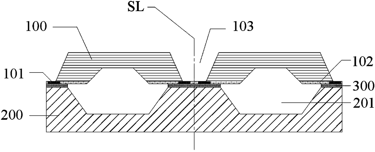
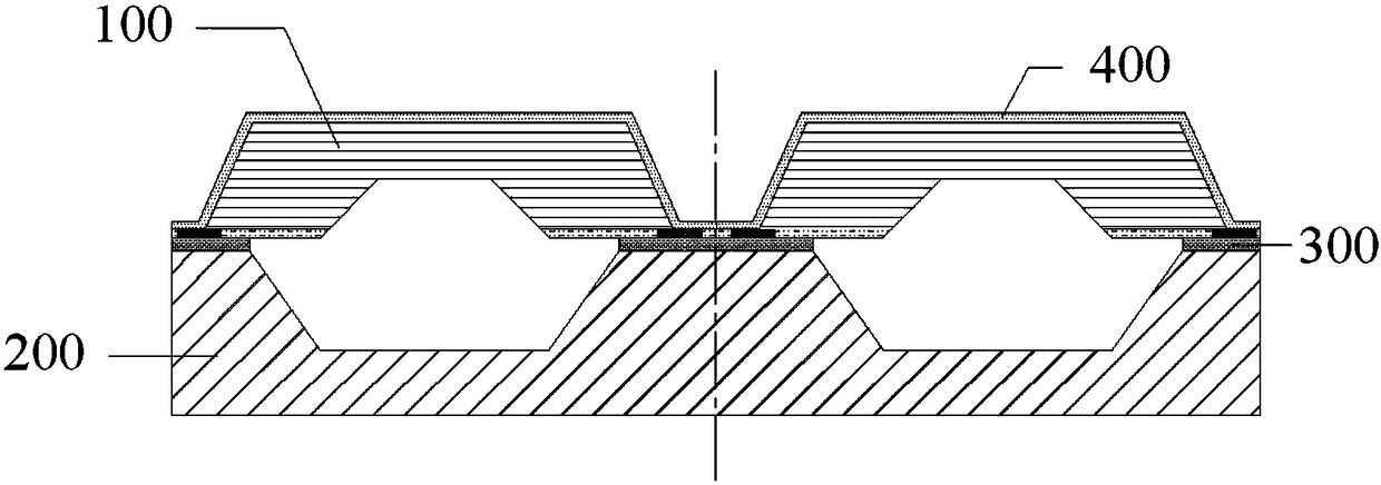
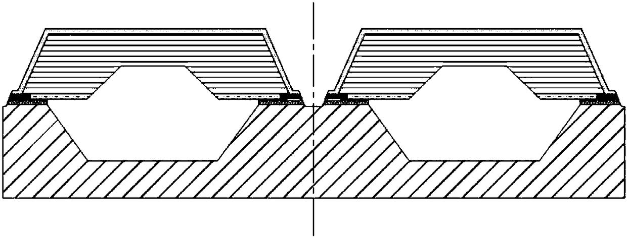
[0037] Such as Figure 7 with Figure 8 As shown, a kind of MEMS hermetic packaging structure, comprises a MEMS chip 100 with welding pad 101 and a cover 200 for sealing this MEMS chip on the edge of a functional surface, the edge of the functional surface of the MEMS chip is connected with the cover The front edge of the MEMS chip is bonded together by a polymer layer 300 of a certain width and thickness, the back side of th...


PUM


Abstract

The invention discloses a MEMS airtight packaging structure and a packaging method thereof, comprising a MEMS chip with welding pads on the edge of the functional surface, a cover for sealing, the functional surface of the MEMS chip and the front edge of the cover through a certain width and The thickness of the polymer layer is bonded together. The surface of the bonding pad of the MEMS chip is covered by the polymer layer. The side of the bonding pad facing the outside of the MEMS chip is connected to the conductive line leading to the back of the MEMS chip. block and conductive line covering. The encapsulation structure achieves good sealing by increasing the metal encapsulation area of ​​the product when forming the conductive circuit, without increasing process steps and costs in the process, and has the advantages of low cost and high reliability.

Description

technical field [0001] The invention relates to the field of wafer-level packaging of semiconductor MEMS chips, in particular to a packaging structure and a packaging method for realizing MEMS airtightness at a metal-wrapped bonding interface. Background technique [0002] With the rise of the Internet of Things and smart mobile terminals, the miniaturization of sensors and system integration requirements make packaging more and more important. Due to the complexity of MEMS packaging, the packaging cost of some MEMS products is as high as 60%. Low-cost and high-performance packaging is an important guarantee for the industrialization of MEMS devices. [0003] MEMS packages can be substrate-based, such as LGA packages, or frame-based, such as QFN packages. More and more MEMS packages are now in wafer-level chip-scale (WLCSP) packages. Among them, image sensors, accelerometers, gyroscopes and other products use 3D WLCSP. This packaging method uses through-silicon via technol...

Claims


Application Information

Patent Timeline
Patent Type & Authority Patents(China)
IPC IPC(8): B81B7/00B81C1/00B81C3/00
CPCB81B7/007B81C1/00698B81C3/001
Inventor 于大全李杨袁礼明翟玲玲
Owner HUATIAN TECH KUNSHAN ELECTRONICS
Learn More