Organic light-emitting diode display having high aperture ratio and method for manufacturing the same

A light-emitting diode and display technology, applied in the direction of diode, semiconductor/solid-state device manufacturing, electric solid-state device, etc., can solve the problems of organic light-emitting diode display time and cost, increased defect generation rate, and reduced output

Inactive Publication Date: 2016-05-25
LG DISPLAY CO LTD
View PDF3 Cites 18 Cited by
  • Summary
  • Abstract
  • Description
  • Claims
  • Application Information

AI Technical Summary

Problems solved by technology

When the number of masking processes increases, the time and cost for manufacturing OLED displays and the defect generation rate increase, thereby reducing yield

Method used


Image

  • Organic light-emitting diode display having high aperture ratio and method for manufacturing the same
  • Organic light-emitting diode display having high aperture ratio and method for manufacturing the same
  • Organic light-emitting diode display having high aperture ratio and method for manufacturing the same

Examples


no. 1 approach

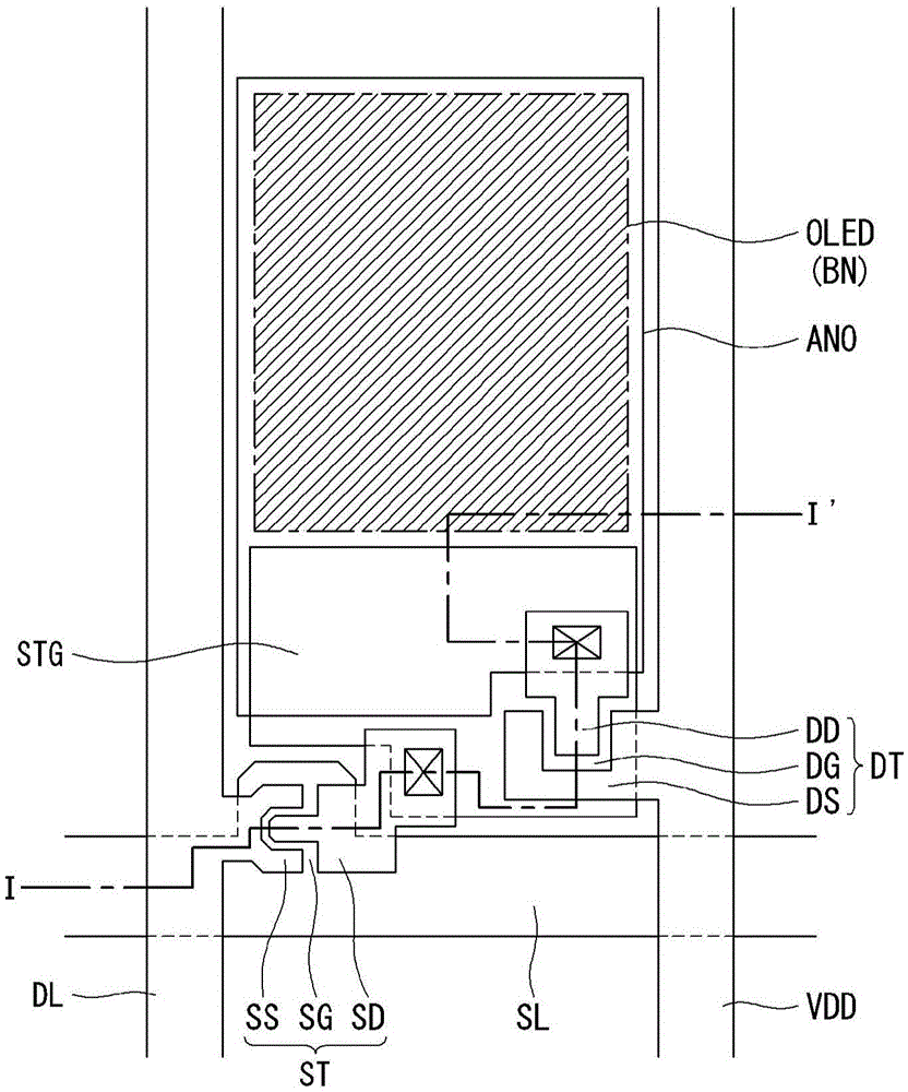
[0036] will refer to Figure 5 with Figure 6 A description is given of the organic light emitting diode display according to the first embodiment of the present invention. Figure 5 is a plan view illustrating the structure of an organic light emitting diode display according to a first embodiment of the present invention, Figure 6 is instantiated along the Figure 5 A cross-sectional view of the structure of the organic light emitting diode display according to the first embodiment of the present invention taken along the line II-II'.

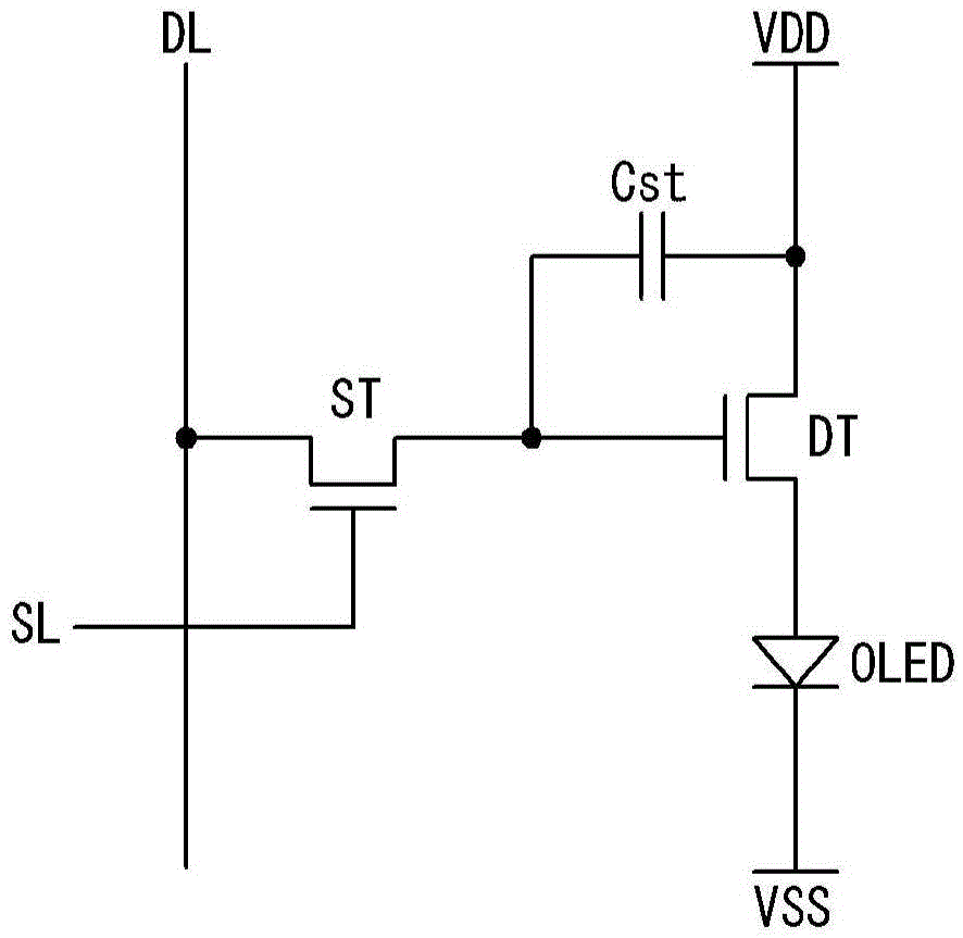
[0037] refer to Figure 5 with Figure 6 , the organic light emitting diode display according to the first embodiment of the present invention includes: a substrate SUB in which a light-emitting area AA and a non-light-emitting area NA are defined; a switch TFTST; a driving TFTDT connected to the switch TFTST; Two storage capacitor electrodes SG2, the second storage capacitor electrode SG2 contact drive TFTDT; storage capacitor STG, the...

no. 2 approach

[0061] will refer to Figure 8 and Figure 9 A description is given of an organic light emitting diode display according to a second embodiment of the present invention. Figure 8 is a plan view illustrating the structure of an organic light emitting diode display according to a second embodiment of the present invention, Figure 9 is instantiated along the Figure 8 A cross-sectional view of the structure of the organic light emitting diode display according to the second embodiment of the present invention taken along the line III-III'.

[0062] refer to Figure 8 and Figure 9 , the organic light emitting diode display according to the second embodiment of the present invention includes: a substrate SUB in which a light-emitting area AA and a non-light-emitting area NA are defined; a switch TFTST; a first storage capacitor electrode SG1, the first storage capacitor The electrode SG1 is connected to the switch TFTST; the driving TFTDT is connected to the switch TFTST; t...


PUM


Abstract

An organic light-emitting diode display can include a substrate in which an emission area and a non-emission area are defined; a first transparent conductive layer, a light shielding layer, a buffer layer and a semiconductor layer sequentially laminated on the non-emission area; a gate electrode superposed on the center region of the semiconductor layer, having a gate insulating layer interposed therebetween; a drain electrode coming into contact with one side of the semiconductor layer, having an interlevel insulating layer covering the gate electrode interposed therebetween, and formed of a second transparent conductive layer and a metal layer laminated thereon; a first storage capacitor electrode disposed under the interlevel insulating layer in the emission area and formed of the first transparent conductive layer; and a second storage capacitor electrode superposed on the first storage capacitor electrode, having the interlevel insulating layer interposed therebetween, and formed of the second transparent conductive layer.

Description

technical field [0001] The present invention relates to an organic light emitting diode display having an improved aperture ratio by forming a storage capacitor in a light emitting region using a transparent conductive material and a method of manufacturing the same. In addition, the present invention relates to an organic light emitting diode display and a method of manufacturing the same for simplifying the manufacturing process by reducing the number of mask processes. Background technique [0002] Recently, various flat panel displays having reduced weight and volume compared with cathode ray tubes have been developed. Such flat panel displays include liquid crystal displays (LCDs), field emission displays (FEDs), plasma display panels (PDPs), electroluminescent devices (ELs), and the like. [0003] EL is classified into inorganic EL and organic light emitting diode displays, and is a self-emitting device having the advantages of high response speed, high luminous effic...

Claims


Application Information

Patent Timeline
Patent Type & Authority Applications(China)
IPC IPC(8): H01L27/32H01L21/77
CPCH10K59/1216H10K59/1201H10K59/38H10K59/124H10K59/126H10K59/1213
Inventor 尹净基金正五白正善南敬真金容玟
Owner LG DISPLAY CO LTD
Why Eureka
Try Eureka