Power semiconductor device

A technology of power semiconductor and main layer, applied in the direction of semiconductor devices, electrical components, thyristors, etc., can solve the problems of high state loss and high on-state loss

Inactive Publication Date: 2016-04-27
ABB TECH AG
View PDF2 Cites 0 Cited by
  • Summary
  • Abstract
  • Description
  • Claims
  • Application Information

AI Technical Summary

Problems solved by technology

[0007] Also, on-state losses are higher than prior art IGCTs due to low voltage MOSFET channel 100 resistance
The base layer 4 is shorted in the EST device so that the thyristor structure enhancement effect is reduced due to hole emission and thus this leads to higher on-state losses

Method used


Image

  • Power semiconductor device
  • Power semiconductor device
  • Power semiconductor device

Examples


Embodiment Construction

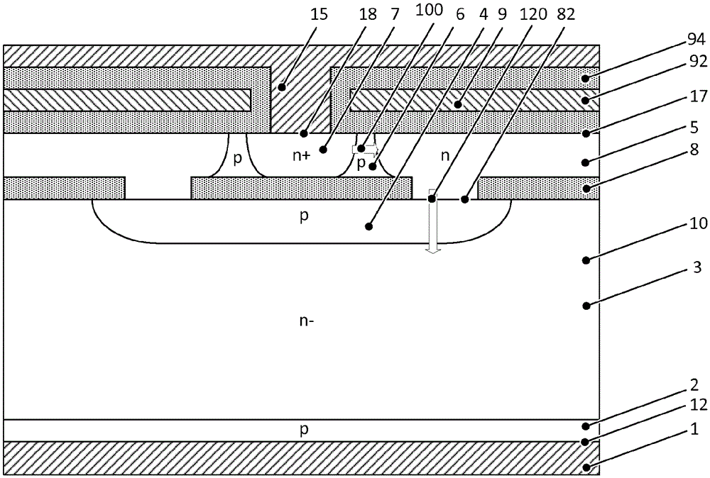
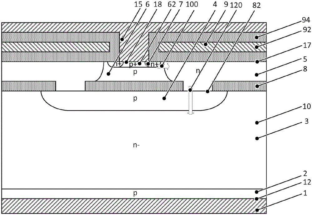
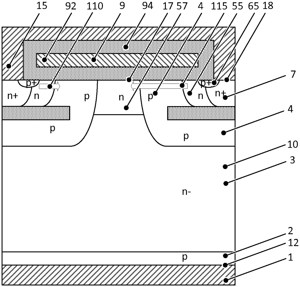
[0038] Such as figure 2 The illustrated inventive power semiconductor device having at least a four-layer structure with layers of a first conductivity type and a second conductivity type different from the first conductivity type comprises a wafer 10 on which an emitter electrode 15 is arranged on On the emitter side 17 of the wafer, and the collector electrode 1 is arranged on the collector side 12 of the wafer opposite the emitter side 17 .

[0039] The wafer comprises n and p doped layers between the collector side 12 and the emitter side 17 . The device includes in the following order:

[0040] -p-doped collector layer 2,

[0041] - a constant low (n-) doped drift layer 3,

[0042] -p-doped base layer 4,

[0043] - a first insulating layer 8 with openings (vias) 82,

[0044] - a highly n-doped emitter layer 5 having a higher maximum doping concentration than the drift layer 3, wherein the emitter layer 5 is in contact with the base layer 4 at the opening 8, and wher...


PUM


Abstract

A power semiconductor device (1) is provided comprising, in the following order: - a collector electrode (1), - a collector layer (2) of a second conductivity type, - a drift layer (3) of a first conductivity type, - a base layer (4) of the second conductivity type, - a first insulating layer (8) having an opening (82), - an emitter layer (5) of the first conductivity type, wherein the emitter layer (5) is in contact with the base layer (4) and separated from the drift layer (3) at least by one of the first insulating layer (8) or the base layer (4), - a body layer (6) of the second conductivity type arranged laterally to the emitter layer (5) and separated from the base layer (4) by the first insulating layer (8) and the emitter layer (5), - a source region (7) of the first conductivity type separated from the emitter layer (5) by the body layer (6), - an emitter electrode (15) contacted by the source region (7). The device further comprises a first layer (65) of the second conductivity type in contact with the emitter electrode (15) and separated from the base layer (4), and a second layer (55) of the first conductivity type arranged between the first layer (65) and the base layer (4) and separated from the emitter layer (5) and the source region (7). A planar MIS gate electrode (9) is arranged laterally from the emitter electrode (15), a corresponding MIS channel being formable between the source region (7), the body layer (6) and the emitter layer (5). A thyristor current path (120) extends between the emitter layer (5), the base layer (4) and the drift layer (3) through the opening (82), and a turn-off MIS channel (110) is formable below the planar MIS gate electrode (9) from the first layer (65), the second layer (55), the base layer (4) to the drift layer (3).

Description

technical field [0001] The present invention relates to power electronics, and more particularly to power semiconductor devices. Background technique [0002] Modes for Realizing the Invention [0003] figure 1 A cross-sectional view of an emitter switching thyristor (EST) comprising a wafer 10 having an emitter side 17 and a collector side 12 on which an emitter electrode 15 and a collector electrode 1 are arranged is shown in . On the emitter side 17 a planar gate electrode 9 is arranged comprising a conductive gate layer 92, a conductive further gate layer 93 and a second insulating layer 94 which connects the gate layers 92 and 93 to the wafer Any layers of the first or second conductivity type in 10 are insulated and insulated from each other. [0004] Similar to in the IGBT, on the emitter side 17 an n+ doped source region 7 extending to the region below the gate layer 91 and a p-doped base layer 4 surrounding the source region 7 are arranged. The source region 7 a...

Claims


Application Information

Patent Timeline
Patent Type & Authority Applications(China)
IPC IPC(8): H01L29/745H01L29/749H01L29/06
CPCH01L29/7455H01L29/0649H01L29/0834H01L29/0839H01L29/0847H01L29/1012H01L29/1095H01L29/41716H01L29/749
Inventor F.鲍尔
Owner ABB TECH AG
Why Eureka
Try Eureka