Graphene room temperature terahertz wave detector and preparation method
A graphene and terahertz technology, applied in the field of terahertz wave detectors, can solve problems such as slow response speed, and achieve the effect of improving miniaturization, high sensitivity, and strong light field coupling ability
- Summary
- Abstract
- Description
- Claims
- Application Information
AI Technical Summary
Problems solved by technology
Method used
Image
Examples
Embodiment 1
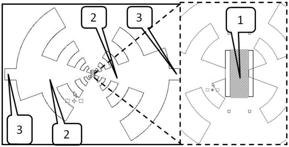
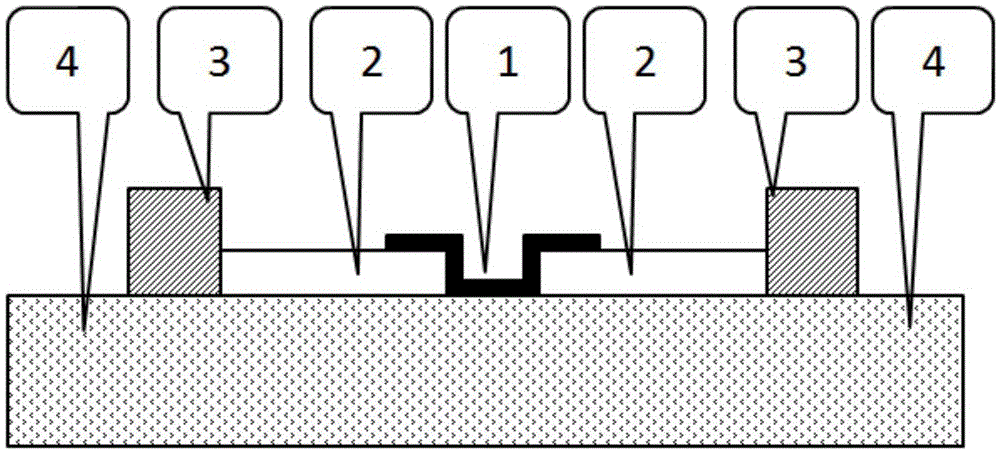
[0044] The thickness of the sapphire substrate is 0.5mm, when the outer diameter of the logarithmic periodic antenna structure is 2mm, the radian is 40°, the thickness is 100, the thickness of the lead electrode 3 is 200nm, and the conductive channel CVD graphene of 80um (concentration is about 10 13 cm -2 , the mobility is about 1000~5000cm 2 V -1 the s -1 ). Under the irradiation of terahertz waves, since the response of the antenna to terahertz waves is related to the polarization direction of the electric field (such as Figure 9 As shown), when the terahertz wave is incident on the front of the detector vertically, and the long side of the logarithmic periodic antenna is about 30° from the direction of the electric field, the responsivity of the antenna is the largest, and the obtained photocurrent is the largest. When the terahertz wave is vertically incident to the front of the detector, and the long side of the antenna is parallel to the antenna, the responsivity o...
Embodiment 2
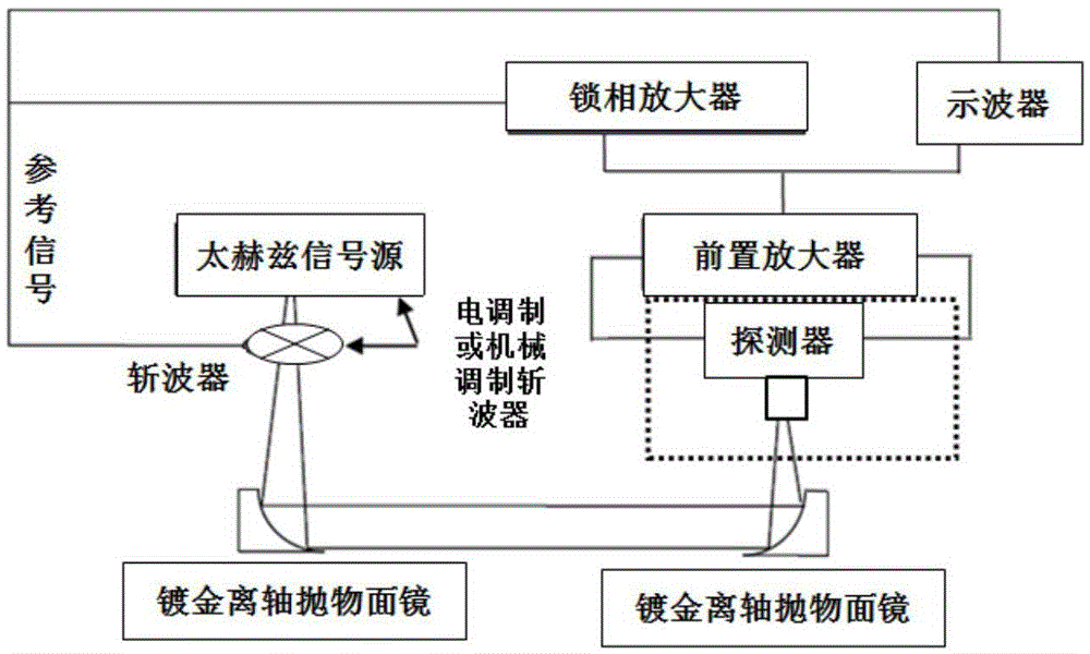
[0046] The thickness of the sapphire substrate is 1mm, when the outer diameter of the logarithmic periodic antenna structure is 1mm, the radian is 50°, the thickness is 100, the thickness of the lead electrode is 200nm, and the conductive channel CVD graphene of 6um (concentration is about 10 13 cm -2 , the mobility is about 1000~5000cm 2 V -1 the s -1 ), the antenna response is related to the polarization direction of the electric field. Similar to Example 1, the antenna response is also related to the bias current on the device. As the current increases, the greater the photoresponsivity and the greater the photocurrent obtained, as Figure 7 As shown, under the premise of a fixed distance of 7cm from the source, the terahertz photoresponsivity of different chopping frequencies is obtained at a bias current of 0.5mA or 1.0mA or 1.5mA or 2.0mA.
Embodiment 3
[0048] The thickness of the sapphire substrate is 0.7mm, when the outer diameter of the logarithmic periodic antenna structure is 2mm, the radian is 40°, the thickness is 100, the thickness of the lead electrode is 200nm, and the conductive channel CVD graphene of 20um (concentration is about 10 13 cm -2 , the mobility is about 1000~5000cm 2 V -1 the s -1 ), the antenna response is related to the polarization direction of the electric field. Similar to Example 1, the antenna response is also related to the distance from the source on the device. As the distance from the source increases, the smaller the photoresponsivity and the smaller the photocurrent obtained, as Figure 8 As shown, the terahertz photoresponsivity of different chopping frequencies is obtained at a fixed bias current of 2mA at a distance of 7cm or 15cm, 25cm or 50cm from the source.
[0049] The parameters of the detector structure vary within a certain range. The graphene room temperature terahertz wave ...
PUM
| Property | Measurement | Unit |
|---|---|---|
| Thickness | aaaaa | aaaaa |
| Outer radius | aaaaa | aaaaa |
| Thickness | aaaaa | aaaaa |
Abstract
Description
Claims
Application Information
 - R&D
- Intellectual Property
- Life Sciences
- Materials
- Tech Scout
- Unparalleled Data Quality
- Higher Quality Content
- 60% Fewer Hallucinations
Browse by: Latest US Patents, China's latest patents, Technical Efficacy Thesaurus, Application Domain, Technology Topic, Popular Technical Reports.
© 2025 PatSnap. All rights reserved.Legal|Privacy policy|Modern Slavery Act Transparency Statement|Sitemap|About US| Contact US: help@patsnap.com


