
A highly integrated communication unit circuit

A communication unit, highly integrated technology, applied in electrical components, transmission systems, etc., can solve the problem of difficulty in reducing the size of the system structure, and achieve the effect of improving the reliability of the circuit, saving costs, and high integration.

Active Publication Date: 2019-01-22
NO 54 INST OF CHINA ELECTRONICS SCI & TECH GRP
View PDF5 Cites 0 Cited by
  • Summary
  • Abstract
  • Description
  • Claims
  • Application Information

AI Technical Summary

Problems solved by technology

It overcomes the problem that the size of the entire system is difficult to reduce due to the electromagnetic compatibility of high-frequency circuits and low-frequency circuits

Method used


Image

  • A highly integrated communication unit circuit
  • A highly integrated communication unit circuit
  • A highly integrated communication unit circuit

Examples


Embodiment Construction

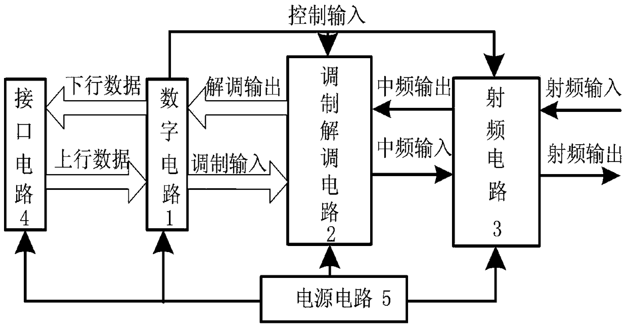
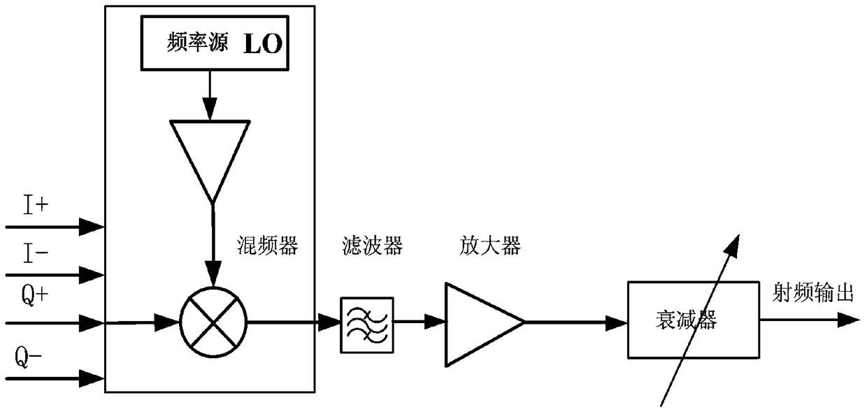
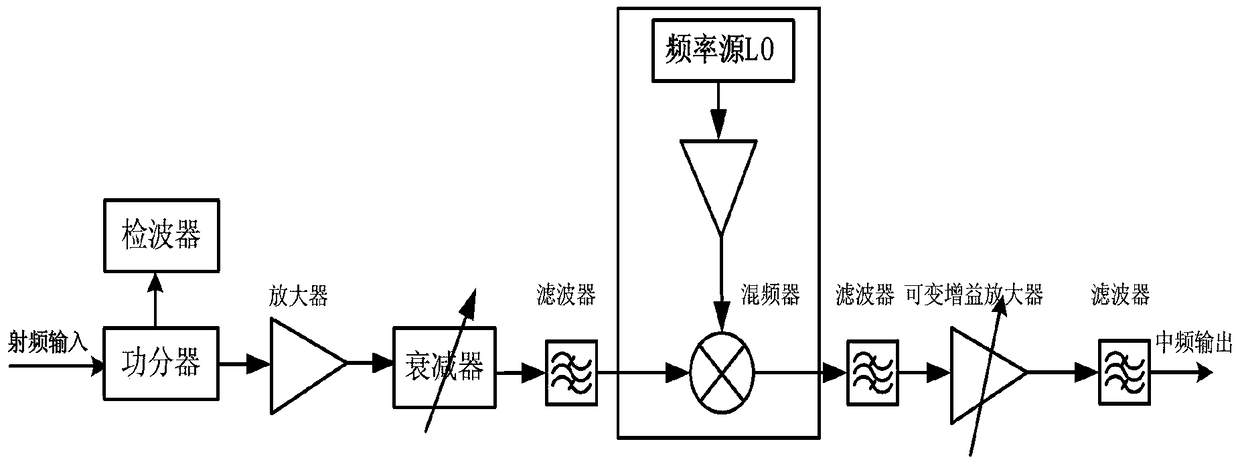
[0021] refer to figure 1 , the present invention is composed of a digital circuit 1, a modulation and demodulation circuit 2, a radio frequency circuit 3, an interface circuit 4, and a power supply circuit 5. figure 1 It is a block diagram of the circuit principle of the present invention. Combining a variety of circuit structures with different functions, using a certain printed board electromagnetic compatibility design method and a highly integrated circuit, the entire communication unit can achieve the characteristics of full functions and small structure size; for the uplink processing of the input communication unit data, the uplink data output port of the interface circuit 4 is connected with the uplink data input port of the digital circuit 1; the uplink data output port of the digital circuit 1 is connected with the modulation signal input port of the modulation and demodulation circuit 2; the modulation and demodulation circuit 2 The modulated signal output port of ...


PUM


Abstract

The invention discloses a highly integrated communication unit circuit, which highly integrates a digital circuit, a modulation and demodulation circuit, a radio frequency circuit, an interface circuit and a power supply circuit on one circuit board. By adopting highly integrated electronic circuits, compact printed board circuit layout, and rationally optimized electromagnetic compatibility design, the electromagnetic compatibility problems of multiple frequencies, multiple signals, and multiple interfaces on one board are solved, and communication is realized. High integration of unit circuit modules. The communication unit is also suitable for different communication frequency bands. Only the frequency band selection filter of the RF circuit needs to be replaced on the hardware. It has the advantages of high integration, small size, light weight, stable and reliable performance, etc., and is very suitable for use in the current communication field. In various communication systems that have strict requirements for miniaturization, power consumption, etc.

Description

technical field [0001] The invention relates to a highly integrated communication unit circuit in the communication field, which is suitable for miniaturized design communication systems with limited volume, weight and power consumption in the microwave communication field. Background technique [0002] With the rapid development of modern aerospace communication and missile-borne communication systems and the emergence of various special-purpose equipment, affected by various factors such as space, weight, and power consumption, there is an urgent need for miniaturized and generalized communication systems . Therefore, the miniaturization and optimization design of communication circuits, the application of highly integrated chips, and the advanced technology level have promoted the miniaturization process of the entire equipment. Integrating digital circuits and analog circuits on one printed board can greatly reduce the size of the device, but the crosstalk between high-...

Claims


Application Information

Patent Timeline
Patent Type & Authority Patents(China)
IPC IPC(8): H04B1/40H04B1/715
CPCH04B1/40H04B1/715H04B2001/7154
Inventor 田丽君冯本勇郭志昆李建强李飞
Owner NO 54 INST OF CHINA ELECTRONICS SCI & TECH GRP
Learn More