Local contact back passivated solar cells

A solar cell and partial contact technology, applied in the field of solar cells, can solve the problems of reduced passivation area, reduced cell efficiency, increased contact resistance, etc., to achieve the effects of increased short-circuit current, improved photoelectric conversion efficiency, and reduced series resistance

Active Publication Date: 2018-10-26
CSI CELLS CO LTD +1
View PDF4 Cites 0 Cited by
  • Summary
  • Abstract
  • Description
  • Claims
  • Application Information

AI Technical Summary

Problems solved by technology

However, these two metallization methods have their own shortcomings: 1. The circular hole design is prone to produce voids in the contact area, which increases the contact resistance and reduces the battery efficiency; 2. The continuous line leads to the contact area between metal and silicon. Larger, resulting in a decrease in the passivation area, on the one hand, it is not conducive to passivation, on the other hand, it leads to more serious surface recombination, which also reduces the efficiency of the battery

Method used


Image

  • Local contact back passivated solar cells
  • Local contact back passivated solar cells
  • Local contact back passivated solar cells

Examples


Embodiment 1

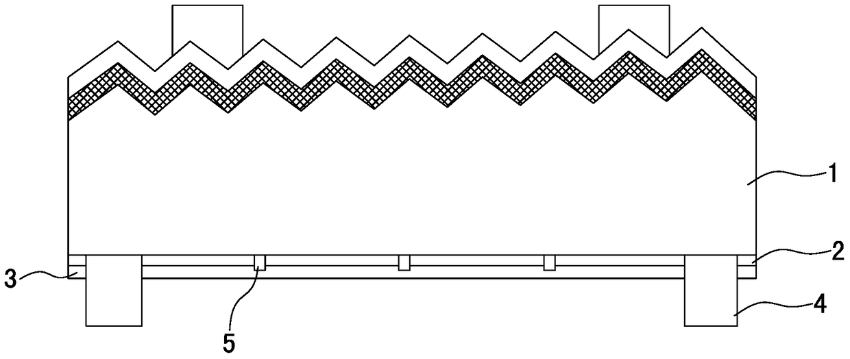
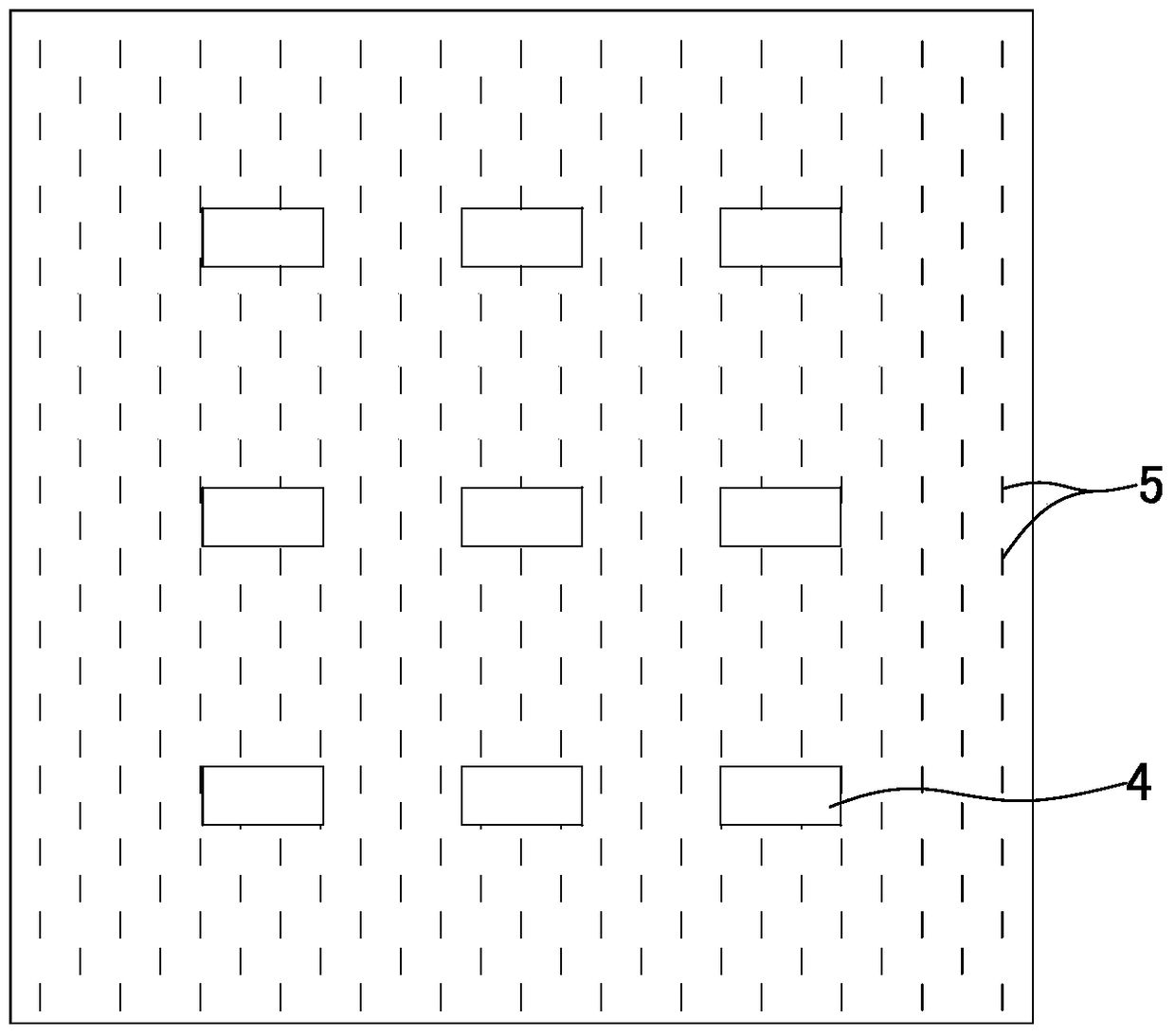
[0034] see Figure 1~3 As shown, a partial contact back passivation solar cell comprises a silicon substrate layer 1, a back passivation film 2 located on the bottom surface of the silicon substrate layer, a back metal layer 3 covering the bottom surface of the back passivation film, and a back passivation film penetrating through the back surface and a plurality of back silver electrodes 4 in the back metal layer and in contact with the bottom surface of the silicon substrate layer, and a plurality of contact regions 5 penetrating through the back passivation film;

[0035] The upper surface of the contact area is in contact with the bottom surface of the silicon substrate layer, the contact area is in the shape of a line segment and arranged in multiple rows parallel to each other, the contact areas in each row are parallel to each other and distributed at intervals, and the contact areas in adjacent rows are staggered distributed;

[0036] In each row of contact areas, the...

Embodiment 2

[0043] see Figure 4 As shown, a kind of partial contact back passivation solar cell, its structure is similar to embodiment one, the difference is:

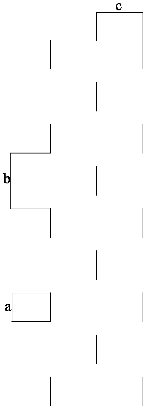
[0044] In each row of contact areas, the length of each contact area is a, and the distance between adjacent contact areas is b; and a is 0.6 mm; b=a, 0.6 mm;

[0045] The spacing c between two adjacent rows of contact areas is 0.8 mm; the spacing between adjacent two rows of contact areas is the same;

[0046] The total area of ​​the contact area accounts for 2.5% of the area of ​​the backside of the silicon wafer.

[0047] In the above technical solution, the width of the contact area is 30 microns.

[0048] The extension direction of the contact area is the same as the extension direction of the back silver electrode.

[0049] The back metal layer is an aluminum layer, and the contact area is a silicon aluminum alloy contact area.


PUM


Abstract

The invention discloses a local contact back passivation solar cell comprising a silicon substrate layer, a back passivation film which is arranged at the bottom surface of the silicon substrate layer, a back metal layer which covers the bottom surface of the back passivation film, multiple back silver electrodes which penetrate through the back passivation film and the back metal layer and are contacted with the bottom surface of the silicon substrate layer, multiple contact regions which penetrate through the back passivation film, and secondary gate electrodes which are arranged at the front surface of the silicon substrate layer and mutually parallel. The contact regions are line-segment-shaped and arranged into multiple rows which are mutually parallel. The contact regions of each row are mutually parallel and arranged in a spacing way. The contact regions in the adjacent rows are arranged in a staggered way. In the contact regions of each row, length of each contact region is 0.1-0.9mm, distance c between the two adjacent rows of contact regions is 0.5-1mm, and the total area of the contact regions is 1-3.5% of the back area of the silicon wafer. The experiment proves that photoelectric conversion efficiency is enhanced for 0.43-0.46% in comparison with the cells in the prior art so that an unexpected technical effect is achieved.

Description

technical field [0001] The invention relates to a partial contact back passivation solar cell, which belongs to the technical field of solar cells. Background technique [0002] Conventional fossil fuels are being exhausted day by day. Among the existing sustainable energy sources, solar energy is undoubtedly the cleanest, most common and most potential alternative energy source. Solar power generation devices, also known as solar cells or photovoltaic cells, can directly convert solar energy into electrical energy. The principle of power generation is based on the photovoltaic effect of semiconductor PN junctions. [0003] With the development of science and technology, a partial contact back passivation solar cell has appeared, which is a newly developed high-efficiency solar cell and has received extensive attention from the industry. Its core is to cover the backlight surface of the silicon wafer with an aluminum oxide or silicon oxide film (also known as the back passi...

Claims


Application Information

Patent Timeline
Patent Type & Authority Patents(China)
IPC IPC(8): H01L31/0216H01L31/0224
CPCH01L31/02167H01L31/022441Y02E10/50
Inventor 吴坚王栩生邢国强
Owner CSI CELLS CO LTD
Why Eureka
Try Eureka