Preparation method for ultrathin chip resistor

A technology of chip resistors and resistors, which is applied in the direction of resistors, resistor manufacturing, and manufacturing resistor chips, etc., can solve the problems of easy damage, etc., and achieve the effect of improving product yield, improving production efficiency, and improving easy breakage

Active Publication Date: 2016-03-16
RALEC TECH KUNSHAN LTD
View PDF3 Cites 0 Cited by
  • Summary
  • Abstract
  • Description
  • Claims
  • Application Information

AI Technical Summary

Problems solved by technology

However, due to the thinner thickness, the thickness of the substrate used in the 01005 type chip resistor is relatively thin, only 0.1mm, and it is easy to be damaged during the production process. Few, the industry is looking for corresponding technological breakthroughs

Method used


Image

  • Preparation method for ultrathin chip resistor
  • Preparation method for ultrathin chip resistor
  • Preparation method for ultrathin chip resistor

Examples


Embodiment 1

[0041] Example 1: A preparation method of an ultra-thin chip resistor, the preparation method comprising the following steps:

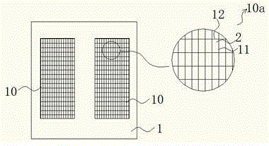
[0042] Substrate segmentation: Divide a substrate 1 into two symmetrical areas 10, laser cut several vertical lines 11 and horizontal lines 12 perpendicular to each other on the two areas 10, and several vertical lines 11 and horizontal lines perpendicular to each other The line 12 divides the two areas evenly into several rectangular grids, and each rectangular grid is a resistor unit 2; figure 2 Middle 10a represents the area 10 on the front side of the substrate;

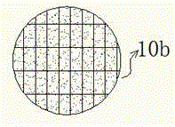
[0043] Step C2: print the conductor layer 20 at each horizontal line 12 on the back side of the substrate 1, see Figure 4 ; image 3 The middle 10b represents the area 10 on the back of the substrate;

[0044] Step C1: Print the conductor layer 21 at each horizontal line 12 on the front side of the substrate 1, see Figure 5 ;

[0045] Step RS: print resistor 22 on the front sid...

Embodiment 2

[0053] Example 2: The difference between this embodiment and Embodiment 1 is that the substrate in this embodiment is a ceramic substrate, the size of the substrate is 60*70mm, and the two symmetrical areas on the substrate are rectangular.

Embodiment 3

[0054] Example 3: The difference between this example and Example 1 is that the thickness of the resistive protective layer in step G1 in this example is 20 ± 10 μm; the thickness of the printed protective layer in step G2 is 20 ± 10 μm; during the electroplating process, The thickness of the nickel plating layer on both sides of each resistor unit is 5.0-6.0 μm; during the electroplating process, the thickness of the zinc plating layer on both sides of each resistor unit is 7.0-8.0 μm. 7.48±1 μm.


PUM

PropertyMeasurementUnit
Sizeaaaaaaaaaa
Thicknessaaaaaaaaaa
Thicknessaaaaaaaaaa

Abstract

The invention discloses a preparation method for an ultrathin chip resistor. The preparation method comprise a step of segmenting a substrate by dividing the substrate into two symmetrical areas and cutting a plurality of mutually perpendicular vertical lines and horizontal lines on each area by using laser, wherein the plurality of mutually perpendicular vertical lines and horizontal lines uniformly segment the two areas into a plurality of rectangular grids, and each rectangular grid is a resistor unit. Thus, the situation that a substrate is prone to fracture in one segmentation during preparation of a thin resistor is improved; and the prepared ultrathin chip resistor has substantially improved yield, and production efficiency is also enhanced.

Description

technical field [0001] The invention relates to the field of electronic component production, in particular to a process method for making ultra-thin chip resistors. Background technique [0002] With the demand for miniaturization, high performance, high reliability, safety and electromagnetic compatibility of electronic equipment in the industrial and consumer electronics market, new requirements are constantly put forward for the performance of electronic circuits, and chip components are further developed towards miniaturization, Multi-layer, large-capacity, high-voltage resistance, integration and high-performance development. The 01005 type thick film chip resistor is the smallest chip resistor in the world, which can greatly reduce the volume of electronic products. With the continuous development of intelligent and miniaturized electronic products, 01005 chip resistors will occupy more and more markets. However, due to the thinner thickness, the thickness of the su...

Claims


Application Information

Patent Timeline
IPC IPC(8): H01C17/00H01C17/065
CPCH01C17/006H01C17/065
Inventor 管春风
Owner RALEC TECH KUNSHAN LTD
Why Eureka
Try Eureka