Current bias circuit

A technology of current bias and current path, applied in the direction of adjusting electrical variables, control/regulation systems, instruments, etc., can solve the problems of consuming circuit area, increasing cost, and large resistance, and achieve resistance area saving, cost reduction, and resistance saving area effect

Active Publication Date: 2016-03-16
SHANGHAI HUAHONG GRACE SEMICON MFG CORP
View PDF5 Cites 10 Cited by
  • Summary
  • Abstract
  • Description
  • Claims
  • Application Information

AI Technical Summary

Problems solved by technology

The resistor R1 used is relatively large, and the large resistor R1 will consume the area of ​​the circuit and increase the cost

Method used


Image

  • Current bias circuit
  • Current bias circuit
  • Current bias circuit

Examples


Embodiment Construction

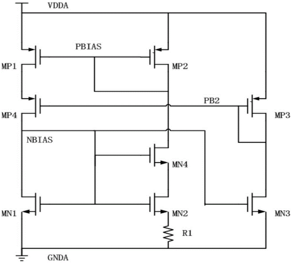
[0028] Such as image 3 Shown is the current bias circuit diagram of the embodiment of the present invention. The current bias circuit in the embodiment of the present invention includes: a first current mirror, a second current mirror and a bias path.

[0029] The first current mirror includes a first PMOS transistor MP1 and a second PMOS transistor MP2 that are mirror images of each other.

[0030] The second current mirror includes a first NMOS transistor MN1 and a second NMOS transistor MN2 that are mirror images of each other.

[0031] The drain current of the first PMOS transistor MP1 is connected to the drain current of the first NMOS transistor MN1 through the third PMOS transistor MP4 to form a first current path.

[0032] The drain current of the second PMOS transistor MP2 is connected to the drain current of the second NMOS transistor MN2 through the third NMOS transistor MN4 to form a second current path.

[0033]The source of the first NMOS transistor MN1 is gr...


PUM


Abstract

The invention discloses a current bias circuit comprising a first current mirror, a second current mirror and a bias path. The first current mirror comprises a first PMOS pipe and a second PMOS pipe working as a mirror image to each other; the second current mirror comprises a first NMOS pipe and a second NMOS pipe working as a mirror image to each other; drain currents of the first PMOS pipe are connected with drain currents of the third PMOS pipe and the first PMOS pipe to form a first current path; drain currents of the second PMOS pipe are connected with drain currents of a third NMOS pipe and the second NMOS pipe to form a second current path; the first PMOS pipe and the third PMOS pipe form a first co-source co-grid structure; the second NMOS pipe and the third NMOS pipe form a second co-source co-grid structure; a bias path provides grids from the first bias voltage to the third PMOS pipe; and a current output end of the bias path is grounded via a first resistor. By the use of the current bias circuit, resistance area can be reduced and cost can be lowered.

Description

technical field [0001] The present invention relates to a semiconductor integrated circuit, in particular to a current bias circuit. Background technique [0002] Current biasing circuits are widely used in integrated circuits, such as figure 1 Shown is the first existing current bias circuit diagram; figure 1 The middle PMOS transistors MP1 and MP2 are mirror images of each other to form a top current mirror, and the NMOS transistors MN1 and MN2 are mirror images of each other to form a bottom current mirror. The PMOS transistors and NMOS transistors of the top current mirror and the bottom current mirror are respectively connected to form two current paths. The resistor R1 is connected between the source of the NMOS transistor MN2 and the ground, and the source of the NMOS transistor MN1 is grounded; the drain and gate of the NMOS transistor MN1 are connected to the gate of the NMOS transistor MN2, and the connection point is the node NBIAS. The gate of the PMOS transist...

Claims


Application Information

Patent Timeline
IPC IPC(8): G05F3/26
CPCG05F3/262
Inventor 邵博闻
Owner SHANGHAI HUAHONG GRACE SEMICON MFG CORP
Why Eureka
Try Eureka