Method for preventing TEM (Transmission Electron Microscope) chip sample from being cracked

A sample and chip technology, which is applied in the field of preventing TEM chip samples from cracking, can solve the problems of low success rate, high cost, and low productivity, and achieve the effect of avoiding the curtain effect and improving the success rate of sample preparation

Active Publication Date: 2016-02-03
SHANGHAI HUALI MICROELECTRONICS CORP
View PDF9 Cites 5 Cited by
  • Summary
  • Abstract
  • Description
  • Claims
  • Application Information

AI Technical Summary

Problems solved by technology

However, there are two main disadvantages of this method. One is that the nano-manipulator equipment is expensive, up to hundreds of thousands of RMB. The other more important thing is that it takes half a day for a very experienced engineer to complete it. The success rate Low, low productivity, high cost

Method used


Image

  • Method for preventing TEM (Transmission Electron Microscope) chip sample from being cracked
  • Method for preventing TEM (Transmission Electron Microscope) chip sample from being cracked
  • Method for preventing TEM (Transmission Electron Microscope) chip sample from being cracked

Examples


Embodiment Construction

[0030] In order to make the above objects, features and advantages of the present invention more comprehensible, specific implementations of the present invention will be described in detail below in conjunction with the accompanying drawings.

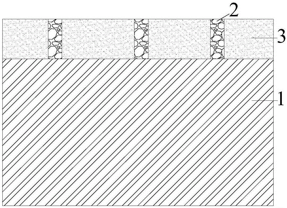
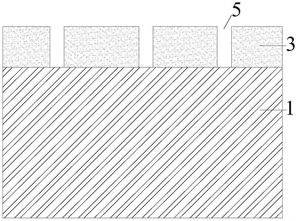
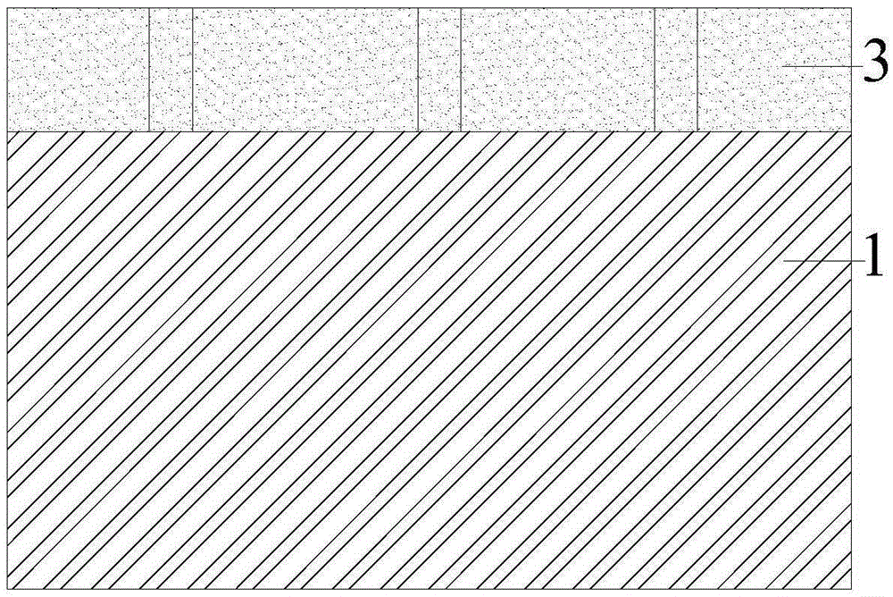
[0031] Please refer to Figure 5 , the invention provides a kind of method that prevents TEM chip sample from cracking, comprises the following steps:

[0032] Step 1: Provide the chip 1, and define the non-observation area and the observation area. In this embodiment, the non-observation area may be the circuit layer or the replacement layer where the gate is located.

[0033] Step 2: Please refer to figure 1 , in the non-observation area, the replacement layer that needs to be replaced is exposed, and the replacement layer can be ground to the replacement layer by chemical mechanical polishing process, or it can be cut first and then used chemical mechanical polishing process to expose the replacement layer, and the replacement laye...


PUM

PropertyMeasurementUnit
thicknessaaaaaaaaaa

Abstract

The invention provides a method for preventing a TEM (Transmission Electron Microscope) chip sample from being cracked. A displacement layer of a material needing to be replaced in a non-observation region of a sample is exposed; the displacement layer is prepared from a conductive material and an insulating material; the conductive material or the insulating material in the displacement layer is removed so that a groove is formed in the displacement layer; the groove is internally filled with a first material; when the first material and an un-removed material are cut by a focusing ion beam, the speeds are the same. The chip prepared by the method can be sequentially used for an existing flow of preparing the TEM sample; in the same displacement layer, the speeds are consistent when all the materials are cut through the focusing ion beam, and a curtain effect is avoided; the method is operated in the non-observation region, influences on an observation region are relatively small, so that the sample preparation success rate is improved and the observation of the sample is not influenced.

Description

technical field [0001] The invention relates to the field of observing chip samples with a transmission electron microscope, in particular to a method for preventing TEM chip samples from breaking. Background technique [0002] Transmission Electron Microscope (TEM for short), referred to as TEM, is to project the accelerated and concentrated electron beam onto a very thin sample, and the electrons collide with the ions in the sample to change the direction, resulting in solid angle scattering, scattering angle The size of the sample is related to the density and thickness of the sample, so images with different light and shade can be formed, and the images will be displayed on imaging devices (such as fluorescent screens, films or photosensitive coupling components) after zooming in and focusing. Nowadays, transmission electron microscopy is widely and increasingly important in various fields including integrated circuit analysis, and FIB (Focused Ion Beam, Focused Ion Beam...

Claims


Application Information

Patent Timeline
Patent Type & Authority Applications(China)
IPC IPC(8): G01N1/28
Inventor 陈强
Owner SHANGHAI HUALI MICROELECTRONICS CORP
Why Eureka
Try Eureka