Vertical hall device
A vertical Hall and device technology, applied in the direction of Hall effect devices, electric solid devices, instruments, etc.
- Summary
- Abstract
- Description
- Claims
- Application Information
AI Technical Summary
Problems solved by technology
Method used
Image
Examples
Embodiment Construction
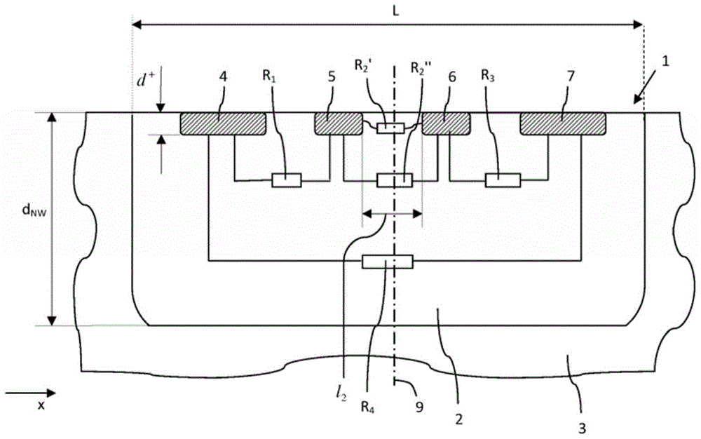
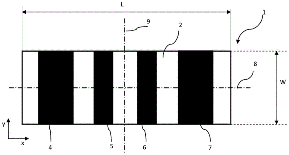
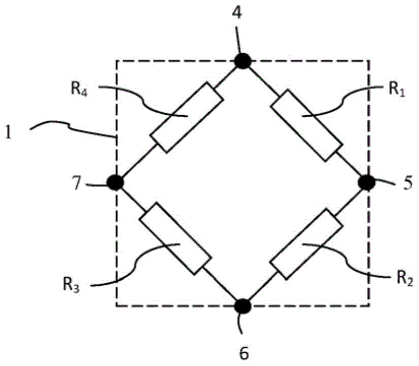
[0056] Figure 4 is a plan view of a first embodiment of a four-contact vertical Hall device 1 according to the present invention. The vertical Hall device 1 is fabricated, for example, by a well-known CMOS process and includes a deep N-well NW embedded in a low-doped P-type substrate 3 (substrate-doped porous silicon (PS) is used). Preferably, the deep N-well NW has a rectangular shape with length L and width W. The vertical Hall device 1 has 4 electrical contacts 4 - 7 arranged at the N-well NW surface and arranged along the first symmetry line 8 , and these electrical contacts are symmetrical with respect to the symmetry plane 9 . The line of symmetry 8 is a straight line and runs orthogonally to the plane of symmetry 9 . Electrical contacts 4-7 are made of highly doped N + area formation. The electrical contacts 4-7 have a generally rectangular shape. The internal contacts 5, 6 have the same length l 6 and the same width W 2 , and the external contacts 4, 5 have the...
PUM
 Abstract
Description
Claims
Application Information
 - R&D
- Intellectual Property
- Life Sciences
- Materials
- Tech Scout
- Unparalleled Data Quality
- Higher Quality Content
- 60% Fewer Hallucinations
Browse by: Latest US Patents, China's latest patents, Technical Efficacy Thesaurus, Application Domain, Technology Topic, Popular Technical Reports.
© 2025 PatSnap. All rights reserved.Legal|Privacy policy|Modern Slavery Act Transparency Statement|Sitemap|About US| Contact US: help@patsnap.com


