


Quick Research
Generate reliable direction feasibility study reports for your R&D in just a few steps.

Technical Q&A
Discover and master advanced knowledge NOW. Basics, ideas, possibilities, all at once.

Find Solutions
As an expert in R&D theories, this can generate solutions to your technical problems instantly.

Evaluate Feasibility
Analyze your overall solution with one click, know your potential R&D risks in advance.

Monitor Landscape
Get weekly tech updates, stay abreast of the latest tech innovations and key insights.
Asymmetric voltage stabilizing circuit used for NAND FLASH
A voltage stabilizing circuit, asymmetrical technology, applied in the direction of adjusting electrical variables, instruments, control/regulation systems, etc., can solve problems such as large overshoot voltage
- Summary
- Abstract
- Description
- Claims
- Application Information
AI Technical Summary
Problems solved by technology
Method used
Image

Examples
Embodiment 1
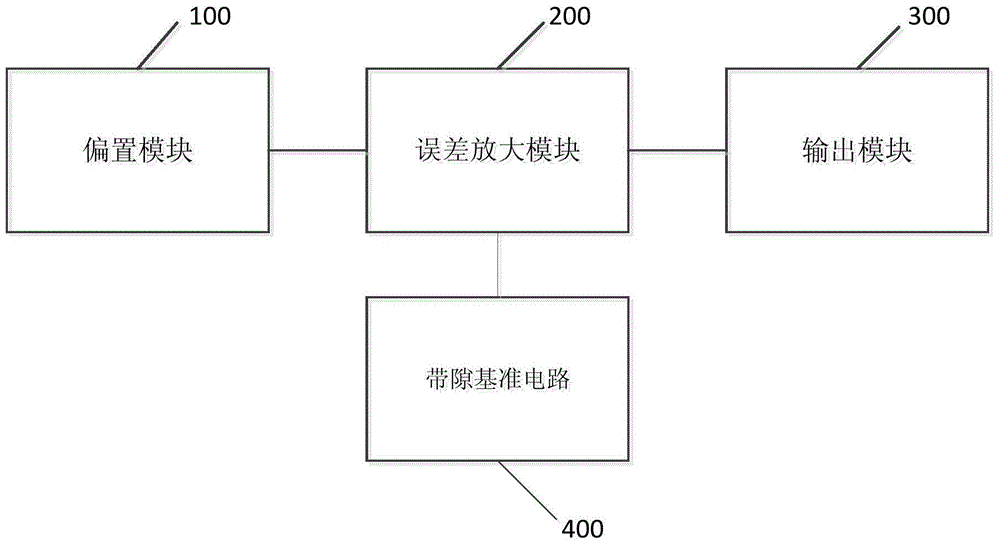
[0040] figure 1 A schematic structural diagram of an asymmetrical voltage stabilizing circuit for NAND FLASH flash memory provided in Embodiment 1 is given.
[0041] Such as figure 1 An asymmetric voltage regulator circuit for NAND FLASH flash memory provided in Embodiment 1 is characterized in that it includes: a bias module 100 , an error amplification module 200 , an output module 300 and a bandgap reference circuit 400 .
[0042] The output terminal of the bias module 100 is electrically connected to the input terminal of the error amplification module 200, and is used to convert the external input voltage into a first bias voltage, a second bias voltage, a third bias voltage and a fourth bias voltage. The bias voltage is input to the error amplifier module 200;
[0043] The output terminal of the error amplification module 200 is electrically connected to the input terminal of the output module 300, and is used to transform the differential signal according to the first...
Embodiment 2
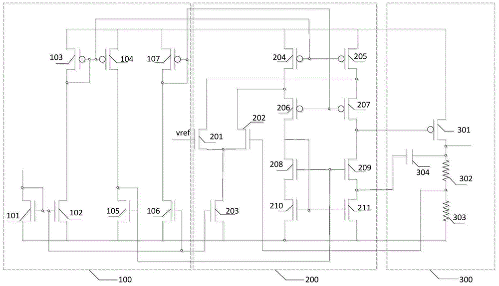
[0051] figure 2 A schematic circuit diagram of an asymmetrical voltage stabilizing circuit for NAND FLASH flash memory provided in Embodiment 2 is given.
[0052] Combine below figure 2 An asymmetrical voltage stabilizing circuit for NAND FLASH flash memory provided in Embodiment 2 is described in detail.
[0053] Embodiment 2 provides an asymmetric voltage regulator circuit for NAND FLASH flash memory, wherein:
[0054] The function of the bias module 100 is to convert the external input voltage into a first bias voltage, a second bias voltage, a third bias voltage and a fourth bias voltage and input them to the error amplification module 200 .
[0055] The bias module 100 includes a first transistor 101 , a second transistor 102 , a third transistor 103 , a fourth transistor 104 , a fifth transistor 105 , a sixth transistor 106 and a seventh transistor 107 .
[0056] Wherein, the first transistor 101 , the second transistor 102 , the fifth transistor 105 and the sixth t...
PUM
 Abstract
Description
Claims
Application Information
 - R&D Engineer
- R&D Manager
- IP Professional
- Industry Leading Data Capabilities
- Powerful AI technology
- Patent DNA Extraction
Browse by: Latest US Patents, China's latest patents, Technical Efficacy Thesaurus, Application Domain, Technology Topic, Popular Technical Reports.
© 2024 PatSnap. All rights reserved.Legal|Privacy policy|Modern Slavery Act Transparency Statement|Sitemap|About US| Contact US: help@patsnap.com