Array substrate, manufacturing method thereof and liquid crystal display panel

A liquid crystal display panel and array substrate technology, which is applied in the direction of instruments, nonlinear optics, optics, etc., can solve the problems of affecting the imaging quality of the panel and increasing the response time of the liquid crystal display panel, so as to improve the problem of large viewing angle deviation and response time Reduce and increase the effect of Tr

Active Publication Date: 2016-01-06
TCL CHINA STAR OPTOELECTRONICS TECH CO LTD +1
View PDF8 Cites 2 Cited by
  • Summary
  • Abstract
  • Description
  • Claims
  • Application Information

AI Technical Summary

Problems solved by technology

[0006] Existing liquid crystal display panels increase the transmittance TR by increasing the thickness of the liquid crystal cell, but the increase in the thickness of the liquid crystal cell will lead to an increase in the response time RT of the liquid crystal display panel, thereby affecting the imaging quality of the panel

Method used


Image

  • Array substrate, manufacturing method thereof and liquid crystal display panel
  • Array substrate, manufacturing method thereof and liquid crystal display panel
  • Array substrate, manufacturing method thereof and liquid crystal display panel

Examples


Embodiment 1

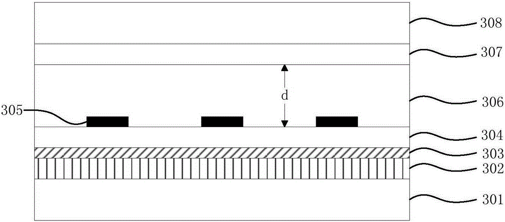
[0045] image 3 A schematic structural diagram of an existing FFS type liquid crystal display panel is shown.

[0046] Such as image 3 As shown, the existing liquid crystal display panel includes: an array substrate, a liquid crystal cell 306 and a CF substrate. Wherein, the array substrate includes: a lower substrate 301 , a first insulating layer 302 , a common electrode 303 , a second insulating layer 304 and a pixel electrode 305 . The CF substrate includes a color filter 307 and a glass substrate 308 . Wherein, the pixel electrode 305 is formed on the second insulating layer 304 . For the liquid crystal cell 306 , its thickness is the distance d between the color filter 307 and the second insulating layer 304 . For the existing FFS liquid crystal display panel, the thickness d of the liquid crystal cell is also its effective thickness. The lower substrate 301 includes structures such as a light-transmitting liner, an insulating layer, and scan lines and / or data line...

Embodiment 2

[0065] Figure 7 A schematic structural diagram of an existing IPS liquid crystal display panel is shown.

[0066] Such as Figure 7 As shown, the existing liquid crystal display panel includes: an array substrate, a liquid crystal cell 704 and a CF substrate. Wherein, the array substrate includes: a lower substrate 701 , an insulating layer 702 and an electrode layer 703 . The CF substrate includes a color filter 705 and a glass substrate 706 . Wherein, the electrode layer 703 is formed on the insulating layer 702 . For the liquid crystal cell 704 , its thickness is the distance d between the color filter 705 and the insulating layer 702 . For the existing IPS liquid crystal display panel, the thickness d of the liquid crystal cell is also its effective thickness.

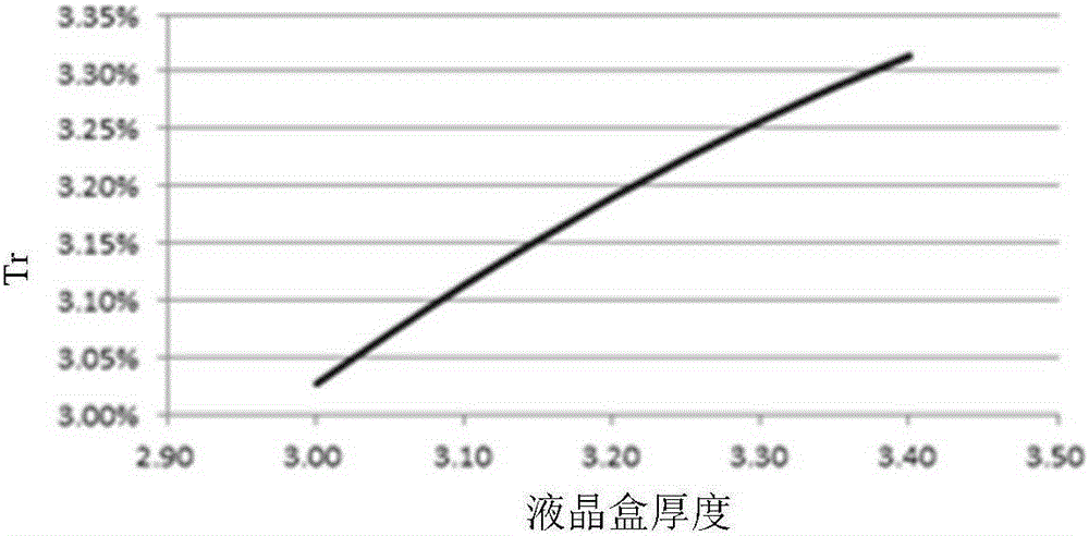
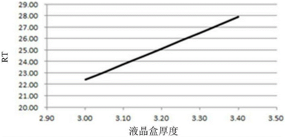
[0067] The existing liquid crystal display panel increases the transmittance Tr of the panel by increasing the thickness of the liquid crystal cell 704 , however, the increase in the thickness of the liquid c...


PUM


Abstract

The invention discloses an array substrate, a manufacturing method thereof and a liquid crystal display panel. The array substrate comprises a first material layer and a first conductive layer formed on the first material layer. The area, not blocked by the first conductive layer, of the first material layer is completely or partially etched in the thickness direction. By means of the array substrate, the effective thickness of a liquid crystal box is increased, so that the panel transmittance is improved; meanwhile, it can be ensured that the response time of the liquid crystal display panel comprising the array substrate is not prolonged.

Description

technical field [0001] The invention relates to the technical field of liquid crystal imaging, in particular, to an array substrate, a manufacturing method thereof, and a liquid crystal display panel. Background technique [0002] Liquid crystal displays have the advantages of low radiation, small size, and low energy consumption. They have gradually replaced traditional cathode ray tube displays and are widely used in products such as flat-screen TVs, personal computers, and mobile display panels. [0003] For a liquid crystal display panel, increasing the transmittance of the liquid crystal display panel can greatly improve the utilization rate of the backlight. Since most of the power consumption of the entire liquid crystal display is the energy consumption of the backlight, increasing the utilization rate of the backlight helps to reduce the energy consumption of the backlight, thereby reducing the power consumption of the entire liquid crystal display. [0004] In add...

Claims


Application Information

Patent Timeline
Patent Type & Authority Applications(China)
IPC IPC(8): G02F1/1339G02F1/1333
CPCG02F1/1333G02F1/1339G02F1/133371G02F1/13439G02F1/133512G02F1/134336
Inventor 唐岳军李亚锋
Owner TCL CHINA STAR OPTOELECTRONICS TECH CO LTD
Why Eureka
Try Eureka