


Quick Research
Generate reliable direction feasibility study reports for your R&D in just a few steps.

Technical Q&A
Discover and master advanced knowledge NOW. Basics, ideas, possibilities, all at once.

Find Solutions
As an expert in R&D theories, this can generate solutions to your technical problems instantly.

Evaluate Feasibility
Analyze your overall solution with one click, know your potential R&D risks in advance.

Monitor Landscape
Get weekly tech updates, stay abreast of the latest tech innovations and key insights.
Preparation method of nanometer clearance and application thereof
A nano-gap, horizontal direction technology, applied in the nanometer field, can solve the problems that the nano-gap cannot meet the application of nano-electrodes, lack of controllability, poor uniformity of the nano-gap, etc.
- Summary
- Abstract
- Description
- Claims
- Application Information
AI Technical Summary
Problems solved by technology
Method used
Image

Examples
preparation example Construction
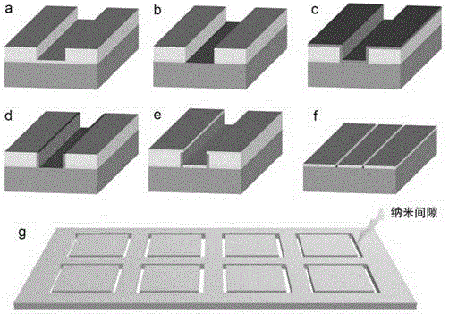
[0026] The invention provides a method for preparing a nano-gap, comprising:
[0027] 1) performing photolithography treatment on the metal thin film in the sample for depositing the first metal thin film to obtain a sample of the first metal thin film protected by part of the photoresist;
[0028] 2) Etching the first metal in the unprotected part of the photoresist in the obtained sample of the first metal thin film partially protected by the photoresist to obtain an etched sample;
[0029] 3) Depositing metal oxide on the etched sample to obtain a sample deposited with metal oxide;
[0030] 4) Etching the metal oxide deposited in the horizontal direction in the sample deposited with the metal oxide to obtain a sample in which the metal oxide deposited in the horizontal direction was removed;
[0031] 5) Depositing a second metal on the sample from which the metal oxide deposited in the horizontal direction has been removed, to obtain a sample for depositing a second metal ...
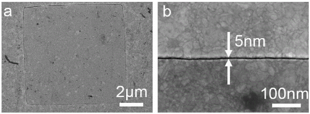
Embodiment 1
[0054] Si and SiO 2 Composite substrate composed of (wherein, the lattice orientation of Si sheet is 111, SiO 2 The thickness of the layer is 300 nanometers) and cut into small pieces of 1 cm×1 cm, ultrasonicated through acetone, absolute ethanol, and deionized water for five minutes respectively, and dried with nitrogen gas for later use to obtain a substrate.
[0055] A 30nm gold film was evaporated on the substrate by electron beam thermal evaporation, and the evaporation rate Obtain the sample of deposited gold film;
[0056] The chloroform solution (wherein, the mass percent concentration of PMMA in the mixed solution of PMMA and chloroform is 4wt%) of 950000PMMAA4 weight-average molecular weight with the speed spin coating of 4000 rev / s on the sample of deposition gold thin film, hot stage 180 ℃ of glue-baking For 4 minutes, a sample coated with photoresist with a thickness of 280 nm was obtained.
[0057] Put the sample spin-coated with PMMA into the electron beam e...
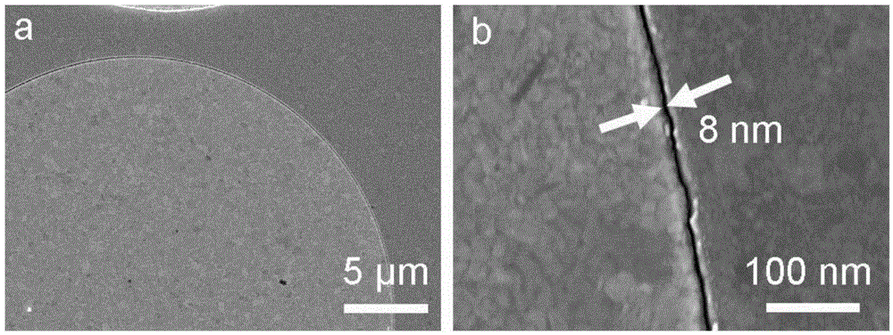
Embodiment 2
[0066] Si and SiO 2 Composite substrate composed of (wherein, the lattice orientation of Si sheet is 111, SiO 2 The thickness of the layer is 300 nanometers) and cut into small pieces of 1 cm×1 cm, ultrasonicated through acetone, absolute ethanol, and deionized water for five minutes respectively, and dried with nitrogen gas for later use to obtain a substrate.
[0067] A 30nm gold film was evaporated on the substrate by electron beam thermal evaporation, and the evaporation rate Obtain the sample of deposited gold film;
[0068] The chloroform solution (wherein, the mass percent concentration of PMMA in the mixed solution of PMMA and chloroform is 4wt%) of 950000PMMAA4 weight-average molecular weight with the speed spin coating of 4000 rev / s on the sample of deposition gold thin film, hot stage 180 ℃ of glue-baking For 4 minutes, a sample coated with photoresist with a thickness of 280 nm was obtained.
[0069] Put the sample spin-coated with PMMA into the electron beam e...
PUM
| Property | Measurement | Unit |
|---|---|---|
| thickness | aaaaa | aaaaa |
| thickness | aaaaa | aaaaa |
| thickness | aaaaa | aaaaa |
Abstract
Description
Claims
Application Information
 - R&D Engineer
- R&D Manager
- IP Professional
- Industry Leading Data Capabilities
- Powerful AI technology
- Patent DNA Extraction
Browse by: Latest US Patents, China's latest patents, Technical Efficacy Thesaurus, Application Domain, Technology Topic, Popular Technical Reports.
© 2024 PatSnap. All rights reserved.Legal|Privacy policy|Modern Slavery Act Transparency Statement|Sitemap|About US| Contact US: help@patsnap.com