
Nanometer silver line conductive overlapping structure and capacitive touch panel

A technology of nano-silver wire and laminated structure, which is applied in the direction of electrical digital data processing, instruments, data processing input/output process, etc., can solve problems such as warping or deformation, and achieve non-slip, simple preparation methods, and warping or the effect of deformation relief

Active Publication Date: 2015-12-30
TPK TOUCH SOLUTIONS (XIAMEN) INC
View PDF7 Cites 19 Cited by
  • Summary
  • Abstract
  • Description
  • Claims
  • Application Information

AI Technical Summary

Problems solved by technology

[0009] In order to overcome the problem of adhesion between the nano-silver wire conductive electrode layer and the substrate, and problems such as warpage or deformation caused by the expansion of the flexible substrate in the film-forming manufacturing process, the invention provides a nano-silver wire Wire conductive laminated structure and capacitive touch panel using the nano-silver wire conductive laminated structure

Method used


Image

  • Nanometer silver line conductive overlapping structure and capacitive touch panel
  • Nanometer silver line conductive overlapping structure and capacitive touch panel
  • Nanometer silver line conductive overlapping structure and capacitive touch panel

Examples


Embodiment Construction

[0032] In order to make the purpose, technical solutions and advantages of the present invention more clear, the present invention will be further described in detail below in conjunction with the accompanying drawings and implementation examples. It should be understood that the specific embodiments described here are only used to explain the present invention, not to limit the present invention.

[0033] When the silver is at the nanoscale, the silver nanowires have good light transmittance and excellent conductivity, and can be well used in touch electrodes of touch panels.

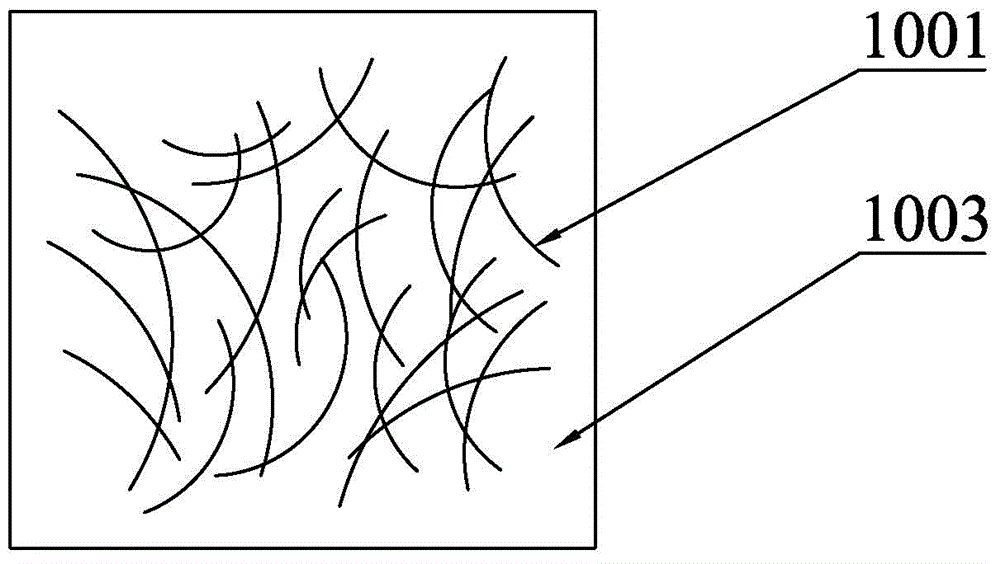
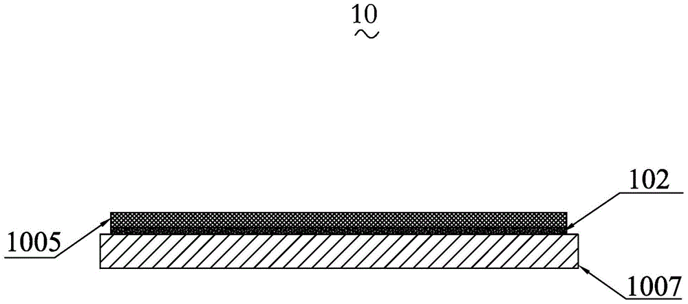
[0034] see figure 1 and figure 2 , is a schematic diagram of the nano-silver wire conductive electrode layer 1005 distributed on the flexible substrate 1007, which includes the flexible substrate 1007 and the nano-silver wire conductive electrode layer 1005 made on the flexible substrate 1007, and the nano-silver wire The wire conductive electrode layer 1005 includes a matrix 1003 and a plurality of...


PUM

PropertyMeasurementUnit
Thicknessaaaaaaaaaa
Square resistanceaaaaaaaaaa
Thicknessaaaaaaaaaa

Abstract

The invention relates to a conductive overlapping structure, in particular to a nanometer silver line conductive overlapping structure. The nanometer silver line conductive overlapping structure comprises a flexible base material, a nanometer silver line conductive electrode layer and an adhesive force increasing layer, wherein the nanometer silver line conductive electrode layer is arranged on the surface of the flexible base material, and the adhesive force increasing layer is arranged between the flexible base material and the nanometer silver line conductive electrode layer and used for increasing the adhesive force between the flexible base material and the nanometer silver line conductive electrode layer. According to an existing nanometer silver line conductive overlapping structure, poor lap joints or shift between nanometer silver lines can influence conductivity of the existing nanometer silver line conductive overlapping structure; by arranging the adhesive force increasing layer, the adhesive force between the nanometer silver line conductive electrode layer and the base material is enhanced. The invention further provides a capacitive touch panel with the nanometer silver line conductive overlapping structure.

Description

【Technical field】 [0001] The invention relates to a conductive laminated structure, in particular to a nano-silver wire conductive laminated structure and a capacitive touch panel using the nano-silver wire conductive laminated structure. 【Background technique】 [0002] With the rapid rise of the touch panel in the communication industry in recent years, especially the booming development of the mobile phone communication industry, the touch panel has become the first-choice product of today's imaging display devices. The touch panels with the highest usage rate are mainly resistive touch panels and capacitive touch panels, but for the sake of controllability, ease of use and surface appearance, most users choose capacitive touch panels as their best choice. Best preferred equipment. [0003] In a capacitive touch panel of a traditional smart phone, the material of the touch electrode is usually indium tin oxide (abbreviated as ITO). ITO has high light transmittance and go...

Claims


Application Information

Patent Timeline
IPC IPC(8): G06F3/044
Inventor 吕正源何小娴李绍张凡忠
Owner TPK TOUCH SOLUTIONS (XIAMEN) INC
Learn More