
Clamp for manufacturing process of photoetching mask plate

A technology of manufacturing process and photolithography mask, which is applied in the field of semiconductor technology, can solve problems such as difficult operation, unbalanced development of photoresist plate, etching and deglue, etc., and achieve the effect of avoiding unbalanced

Active Publication Date: 2015-12-30
SHANGHAI INST OF MICROSYSTEM & INFORMATION TECH CHINESE ACAD OF SCI
View PDF9 Cites 5 Cited by
  • Summary
  • Abstract
  • Description
  • Claims
  • Application Information

AI Technical Summary

Problems solved by technology

[0006] 1. It is not easy to operate, especially in the production of large-size photolithography plates
[0007] 2. When entering and taking out the solution, there is a time difference between the corners of the photoresist plate, which may easily cause the uneven development, etching and glue removal of the photoresist plate

Method used

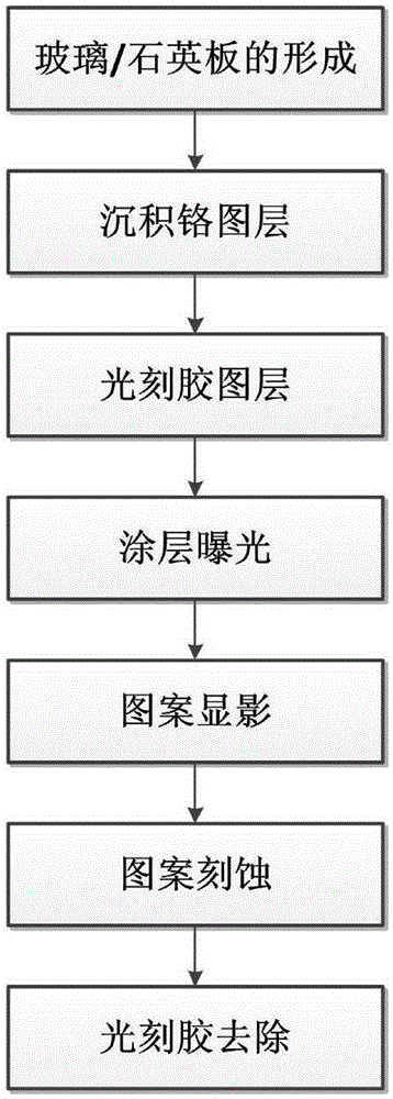

Image

  • Clamp for manufacturing process of photoetching mask plate
  • Clamp for manufacturing process of photoetching mask plate

Examples


Embodiment Construction

[0019] Below in conjunction with specific embodiment, further illustrate the present invention. It should be understood that these examples are only used to illustrate the present invention and are not intended to limit the scope of the present invention. In addition, it should be understood that after reading the teachings of the present invention, those skilled in the art can make various changes or modifications to the present invention, and these equivalent forms also fall within the scope defined by the appended claims of the present application.

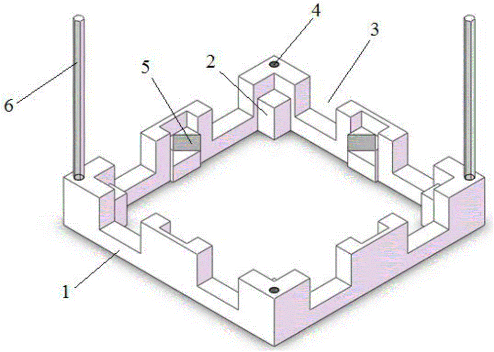
[0020] Embodiments of the present invention relate to a fixture for a photolithographic mask making process, such as figure 2 As shown, it includes a main body part 1, the main body part 1 is a rectangular frame structure; the inner side of the four corners of the main body part 1 is provided with supporting columns 2, and the periphery of the main part 1 is provided with eight notches 3 , eight notches 3 are equally spaced a...


PUM


Abstract

The invention relates to a clamp for the manufacturing process of a photoetching mask plate. The clamp comprises a body part which is of a rectangular framework structure. Supporting column bodies are arranged on the inner sides of the four corners of the body part. A plurality of notches are formed in the periphery of the body part. Threaded holes used for mounting lifting rods are further formed in the four corners of the body part. By the adoption of the clamp, developing, etching and removing of photoresist in the manufacturing process of the mask plate and cleaning of the mask plate can be made more convenient.

Description

technical field [0001] The invention relates to the technical field of semiconductor technology, in particular to a fixture used in the process of making a photolithography mask, which is suitable for developing, etching, degumming and cleaning the photolithography mask. Background technique [0002] The photolithography process is a very important process in the semiconductor process. It is a process used to create patterns on the surface of different devices and circuits. Photolithography determines the critical dimensions and relative positions of the devices. Errors in the photolithography process can cause pattern distortion or poor registration, which can ultimately translate into an impact on the electrical characteristics of the device. In fact, since lithography needs to complete 5 layers to 20 layers or more in the wafer production process, the accuracy of lithography process is particularly important in semiconductor process. [0003] A photolithographic mask is...

Claims


Application Information

Patent Timeline
Patent Type & Authority Applications(China)
IPC IPC(8): G03F1/68
Inventor 孙浩闵文超佟瑞张祁莲丁惠凤钱蓉孙晓玮
Owner SHANGHAI INST OF MICROSYSTEM & INFORMATION TECH CHINESE ACAD OF SCI
Learn More