A kind of radio frequency identification label preparation method based on film technology
A technology of radio frequency identification tags and thin film technology, which is applied in the field of semiconductor integrated circuits, can solve the problems of large and difficult radio frequency identification tags, and achieve the effects of increasing the application range, reducing costs, and reducing costs
- Summary
- Abstract
- Description
- Claims
- Application Information
AI Technical Summary
Problems solved by technology
Method used
Image
Examples
Embodiment 1
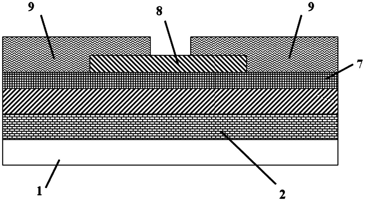
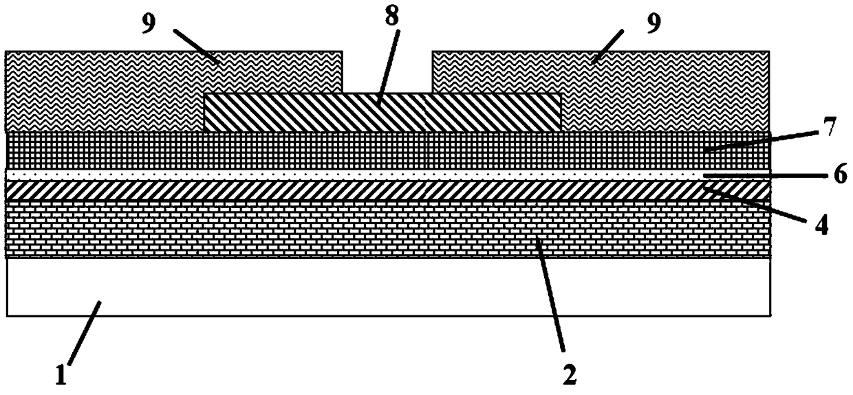
[0055] A method for preparing a radio frequency identification tag based on thin film technology. The radio frequency identification tag consists of an antenna, an analog front-end circuit, a clock and a digital logic circuit, and an EEPROM storage circuit. The EEPROM storage circuit includes a storage device and a peripheral read-write circuit. Among them, the analog front-end circuit, clock and digital logic circuit, and EEPROM peripheral read-write circuit are composed of conventional thin-film transistors, while the EEPROM storage device is composed of storage thin-film transistors. Conventional thin-film transistors adopt an etch-stop structure, such as figure 1 As shown, the substrate 1 is a glass substrate or a flexible substrate, the gate electrode 2 is made of conventional Mo, deposited by physical sputtering, and patterned by wet etching, and its thickness is 200nm; the gate insulating layer is made of SiNx / SiO 2 Stacked structure (including 3, 4, 5 and 6), using pla...
Embodiment 2
[0065] Embodiment 2 is a method for preparing a radio frequency identification tag based on a thin film process. The radio frequency identification tag is composed of an antenna, an analog front-end circuit, a clock and a digital logic circuit. Among them, the analog front-end circuit, the clock and the digital logic circuit are composed of conventional thin film transistors. Conventional thin-film transistors adopt an etch-stop structure, such as figure 1 As shown, the substrate 1 is a glass substrate, the gate electrode 2 is made of conventional Mo, deposited by physical sputtering, and patterned by wet etching, and its thickness is 200nm; the gate insulating layer is made of SiNx / SiO 2 Stacked structure (including 3, 4, 5 and 6), using plasma enhanced chemical vapor deposition, dry etching patterning, wherein the thickness of SiNx is 250nm, SiO 2 The thickness of the active layer 7 is 50nm; the active layer 7 is made of semiconductor material, deposited by radio frequency ...
Embodiment 3
[0072] Embodiment 3 is a method for preparing a radio frequency identification tag based on a thin film process. The radio frequency identification tag consists of an analog front-end circuit, a clock and a digital logic circuit, and an EEPROM storage circuit. The EEPROM storage circuit includes a storage device and a peripheral read-write circuit. Among them, the analog front-end circuit, clock and digital logic circuit, and EEPROM peripheral read-write circuit are composed of conventional thin-film transistors, while the EEPROM storage device is composed of storage thin-film transistors. Conventional thin-film transistors adopt an etch-stop structure, such as figure 1 As shown, the substrate 1 is a glass substrate, the gate electrode 2 is made of conventional Mo, deposited by physical sputtering, and patterned by wet etching, and its thickness is 200nm; the gate insulating layer is made of SiNx / SiO 2 Stacked structure (including 3, 4, 5 and 6), using plasma enhanced chemical...
PUM
 Abstract
Description
Claims
Application Information
 - R&D
- Intellectual Property
- Life Sciences
- Materials
- Tech Scout
- Unparalleled Data Quality
- Higher Quality Content
- 60% Fewer Hallucinations
Browse by: Latest US Patents, China's latest patents, Technical Efficacy Thesaurus, Application Domain, Technology Topic, Popular Technical Reports.
© 2025 PatSnap. All rights reserved.Legal|Privacy policy|Modern Slavery Act Transparency Statement|Sitemap|About US| Contact US: help@patsnap.com


