Silicon-based OLED display pixel preparation method

A display pixel and silicon-based technology, applied in semiconductor/solid-state device manufacturing, electrical components, electric solid-state devices, etc., can solve the problems of insufficient dimensional accuracy and positioning accuracy of RGB pixel areas, unreasonable color mixing ratio, and color distortion of display images, etc. , to achieve normal image color, reduce sheet resistance, and improve performance

Active Publication Date: 2015-12-16
深圳市向阳新能源科技有限公司
View PDF4 Cites 4 Cited by
  • Summary
  • Abstract
  • Description
  • Claims
  • Application Information

AI Technical Summary

Problems solved by technology

[0005] For this reason, the technical problem to be solved by the present invention is that the size accuracy and positioning accuracy of the RGB pixel area in the existing OLED display equipment are insufficient, resulting in unreasonable color mixing ratio and distorted color of the display image. Preparation method of silicon-based OLED display pixel with reasonable color mixing ratio

Method used


Image

  • Silicon-based OLED display pixel preparation method

Examples


Embodiment

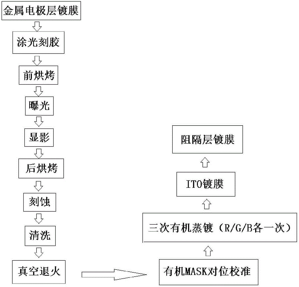
[0033] Such as figure 1 As shown, this embodiment provides a method for manufacturing a silicon-based OLED display pixel, which includes a pixel backplane process and an organic light-emitting layer process, wherein the pixel backplane process includes:

[0034] (1) Metal electrode layer coating is carried out on the monocrystalline silicon substrate, and the substrate pretreatment is carried out before the coating: the monocrystalline silicon substrate is ultrasonically cleaned with deionized water for 2 minutes at 80 ° C in an ultrasonic cleaning device, and then The substrate was rinsed with deionized water at a speed of 1500rpm / min for 1min, and then dried at a high speed of 2500rpm for 1min after cleaning, then put into a nitrogen protection oven and baked for 3min. Using magnetron sputtering coating equipment, Ti / Al / Pt three-layer metal stacked electrodes were fabricated sequentially, with thicknesses of and The coating rate is and Obtain a metal electrode layer;...


PUM


Abstract

The invention discloses a silicon-based OLED display pixel preparation method comprising a pixel backplane process and an organic light-emitting layer process. The pixel backplane process comprises the following steps: (1) coating a metal electrode layer of a substrate; (2) applying photoresist; (3) exposing; (4) developing; (5) etching; (6) cleaning; and (7) vacuum annealing. The organic light emitting layer process comprises the following steps: (8) organic mask alignment and calibration; (9) three times of organic evaporation; (10) ITO coating; and (11) blocking layer coating. Organic mask alignment and calibration is carried out before each organic light-emitting pixel unit evaporation, so that coating cross-interference between different pixel units is avoided. A gap is left between an organic mask and a pixel electrode in the z direction, which prevents pollution to the pixel electrode or the pixel units after evaporation. Meanwhile, as the size and location of a prepared organic light-emitting pixel unit are accurate, the color mixture ratio of three colors is excellent, and images are normal in color and distortion-free.

Description

technical field [0001] The invention belongs to the technical field of organic light-emitting display, and in particular relates to a method for preparing a silicon-based OLED display pixel. Background technique [0002] With the development of multimedia technology, the performance requirements of flat panel display devices are getting higher and higher. In recent years, the following three main display technologies have been developed: plasma display, field emission display and organic electroluminescence display. Among them, the organic electroluminescence display is a display device based on an organic light emitting diode (Organic Light Emitting Diode, referred to as OLED), which has the characteristics of fast response speed, high contrast ratio, and wide viewing angle. In addition, the OLED panel has the characteristics of self-illumination and does not need to use a backlight panel, so the cost of the backlight module is saved, and it is lighter and thinner than the ...

Claims


Application Information

Patent Timeline
Patent Type & Authority Applications(China)
IPC IPC(8): H01L51/56H01L27/32
CPCH10K59/35H10K71/00
Inventor 李海萍
Owner 深圳市向阳新能源科技有限公司
Why Eureka
Try Eureka