
ESD protection device and manufacturing method thereof

A manufacturing method and device technology, applied in semiconductor/solid-state device manufacturing, electric solid-state devices, semiconductor devices, etc., can solve the problems of large conductive area, setting height restrictions, and inconvenient overall layout of capacitors, etc.

Inactive Publication Date: 2015-11-25
SEMICON MFG INT (SHANGHAI) CORP
View PDF3 Cites 3 Cited by
  • Summary
  • Abstract
  • Description
  • Claims
  • Application Information

AI Technical Summary

Problems solved by technology

[0007] However, due to the limitation of the design structure, the capacitor is designed on the substrate of the ESD protection device, and the setting height will be limited, which makes the overall layout of the capacitor very inconvenient, and the conductive area is large, and the ESD current that can be withstand in a unit area is relatively small. small and large degrades the performance of ESD protection devices

Method used

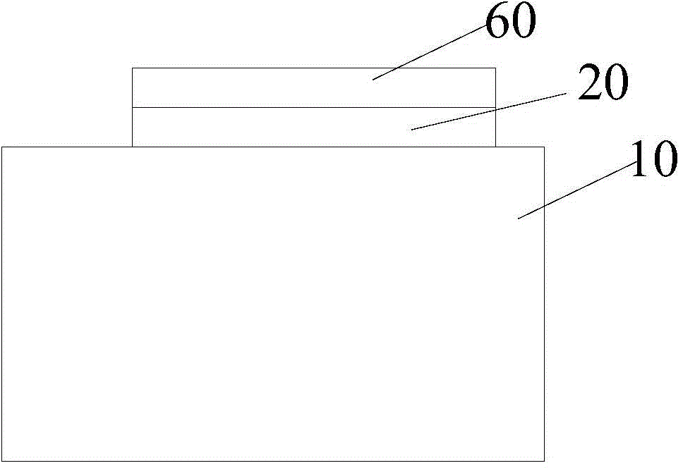
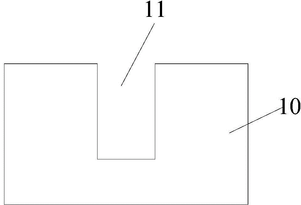
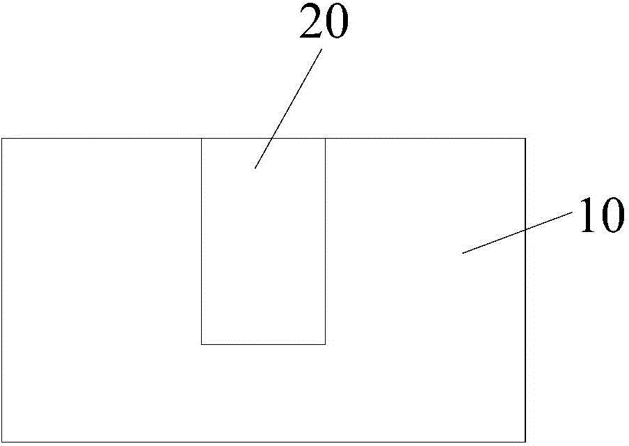

Image

  • ESD protection device and manufacturing method thereof
  • ESD protection device and manufacturing method thereof
  • ESD protection device and manufacturing method thereof

Examples


Embodiment Construction

[0038] It should be pointed out that the following detailed description is exemplary and intended to provide further explanation to the present application. Unless defined otherwise, all technical and scientific terms used herein have the same meaning as commonly understood by one of ordinary skill in the art to which this application belongs.

[0039] It should be noted that the terminology used here is only used to describe specific implementations, and is not intended to limit the exemplary implementations according to the present application. As used herein, unless the context clearly indicates otherwise, the singular form is also intended to include the plural form. In addition, it should also be understood that when the terms "comprising" and / or "comprising" are used in this specification, it indicates There are features, steps, operations, means, components and / or combinations thereof.

[0040]For the convenience of description, spatially relative terms may be used her...


PUM

PropertyMeasurementUnit
Depthaaaaaaaaaa
Groove depthaaaaaaaaaa

Abstract

The invention provides an ESD protection device and a manufacturing method thereof. The ESD protection device comprises a capacitor. The capacitor comprises a substrate which is provided with a groove, an insulating dielectric layer which is formed in the groove and has an accommodation groove, a conductive part which is formed in the accommodation groove formed by the insulating dielectric layer. According to the ESD protection device provided by the invention, the area of the capacitor in the ESD protection device is small, and the performance of the ESD protection device is improved.

Description

technical field [0001] The present application relates to the field of semiconductor devices, in particular, to an ESD protection device and a manufacturing method thereof. Background technique [0002] Static electricity is an objectively existing natural phenomenon, which can be produced in many ways, such as contact, friction, induction between electrical appliances, etc. Static electricity has the characteristics of long-term accumulation, high voltage, low power, low current and short action time. Static electricity causes serious harm in many fields. Frictional electrification and human body static electricity are two major hazards in the electronics industry, which often cause unstable operation or even damage of electronic and electrical products. [0003] For electronic products, there are two types of damage and damage caused by electrostatic discharge: sudden damage and potential damage. The so-called sudden damage refers to the serious damage of electronic devi...

Claims


Application Information

Patent Timeline
IPC IPC(8): H01L27/02H01L21/02
Inventor 魏琰
Owner SEMICON MFG INT (SHANGHAI) CORP
Learn More